
Source: Knowles Precision Devices blog
Product durability and accelerated life cycle testing are all methods of determining the reliability of a product before release. By subjecting the capacitor to elevated conditions far beyond its normal operational ranges, we seek to discover any defects or points of failure to better inform customers about the limitations of the unit.
Burn-In Testing
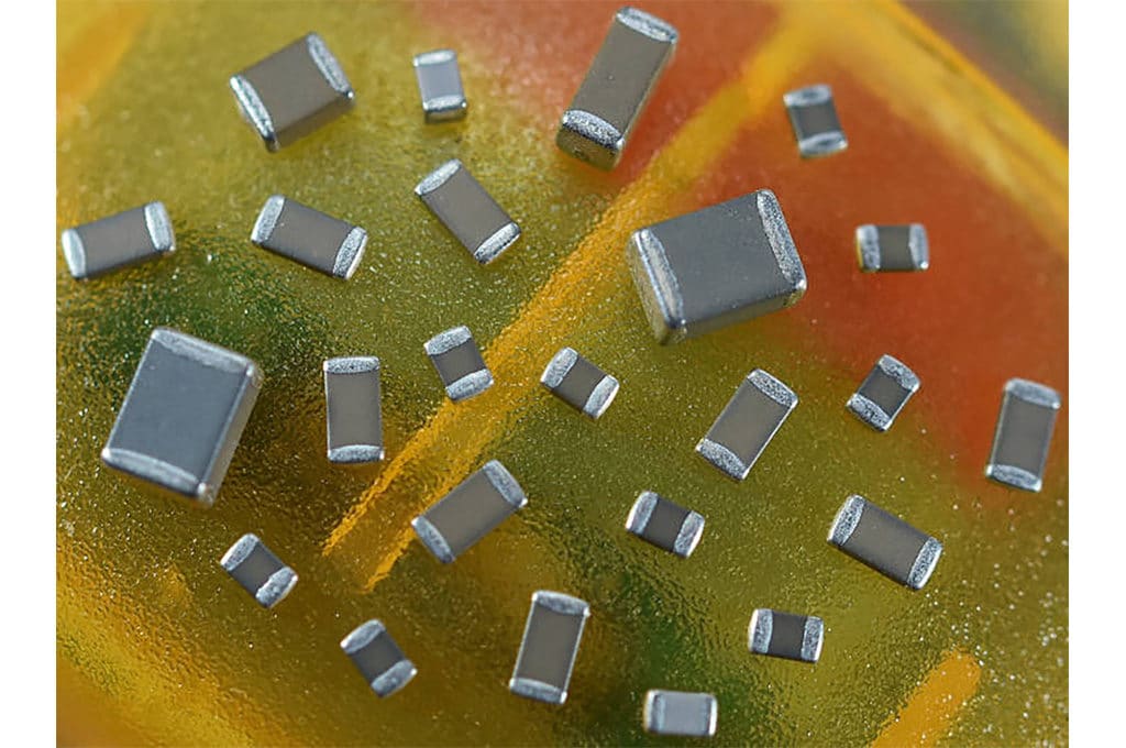
Dielectric formulations and chip capacitors are often tested for reliability under voltage and temperature for specified time periods, a process referred to as burn-in or voltage conditioning.The specifications applicable to burn-in of multilayer ceramic capacitors (MLCCs) are MIL-C-55681, MIL-C-123 and MIL-C-49467. Burn-in may also be performed to particular customer specifications. We typically use a test voltage that is twice the working voltage rating of the device, at 85°C or 125°C for a duration of 96, 100, or 168 hours of test time.
Burn-in is accomplished by loading the units in a fixture, usually a printed circuit board (PCB) which connects to a power supply with access to the rear wall of a standard oven. Units are monitored for current leakage under voltage and temperature stress, either individually or in tandem, with measurement of leakage from a group of a hundred units typically. Tandem testing is more rapid and used to mass-produce burned-in product. Sophisticated test equipment is used with automated data monitoring to record the location and time of test cycle failures.
Chip capacitors destined for high reliability testing are often designed with an added margin of safety, namely maximization of the dielectric thickness, and tested extensively for electrical properties prior to burn-in (e.g., capacitance, dissipation factor, and insulation resistance). This pre-test data is compared to the post burn-in data to evaluate the reliability of the components.
Failure Modes for Burn-In Testing
Capacitors which fail burn-in usually lose resistivity at the elevated temperature and voltage, either catastrophically or gradually with time, resulting in insulation resistance (IR) rejects. The failure rate is usually inversely proportional with time, such that more failures are observed earlier in the test cycle.
However, excellent electrical properties at 25°C may not guarantee good performance during life cycle testing for several reasons:
Poor dielectric properties: Ceramic dielectrics with elevated IR at room temperature may nevertheless experience excessive loss of resistivity at 125°C due to improper formulation. This causes the charge carriers to become mobile and develop a leakage current, decreasing the IR below specifications.
Poor microstructure: Voids, cracks or delaminations within the chip structure undermine the intrinsic resistivity of the material, providing leakage paths conducive to failure. Experience has shown that despite rigorous testing, units with delaminations may still perform adequately, while failures may be observed in units with apparent “excellent” This is because defects that happen to straddle the electrode array are more conducive to eventual degradation under voltage and temperature.
A second failure mode independent of the above reasons is degradation of the capacitance value and/or dissipation factor (DF) of the chip capacitor, when the post burn-in data does not correlate well to the original test data.
Class I non-ferroelectric dielectrics do not exhibit capacitance aging with time, temperature or voltage. Therefore, any burn-in induced capacitance change in Class I chips is associated with mechanical failure, such as cracking which isolates electrode layers.
Class II ferroelectric dielectrics, on the other hand, may display capacitance and DF variations after burn-in without mechanical failure, since these dielectrics are time-, temperature-, and voltage-dependent. Most notably, the accelerated aging of the dielectric constant under burn-in conditions must be considered (e.g., in comparison to pre burn-in data performed on de-aged units) for proper interpretation of results. Units under test may be exposed to three very different aging scenarios, depending on the method used to terminate the life test:
- Procedure 1:The voltage is removed while the units are at temperature, and temperature is maintained with no bias for a minimum of one hour. Under this condition, total de-aging of capacitors occurs, and units will display minimal (positive or negative) capacitance change with respect to the original pre-burn-in values.
- Procedure 2:Capacitors remain under DC bias while the oven is permitted to cool to room temperature. This in effect is a voltage conditioning process and the units will therefore age with respect to the original test data (e.g., -7.0% ΔC).
- Procedure 3:The voltage is removed at the burn-in temperature, and the units subsequently taken from the oven and allowed to air cool to room temperature. In this case, the units do not fully age during the cooling cycle as in procedure 2, nor do they totally de-age as in procedure 1. The components thus experience a partial aging only (e.g., -3.5% ΔC).
The %ΔC values given as examples for the post burn-in data above are typical of some Mid-K Class II dielectrics. High-K less stable dielectrics may experience more radical capacitance changes, as these materials have a typical aging rate of 5% per decade hour, which is three times the average rate of X7R formulations. These considerations clearly indicate that procedure 1 only should be followed for termination of the life test for proper evaluation of performance of Class II dielectrics.
In addition to burn-in, high reliability testing often involves other performance tests per MIL-C-55681 or to customer specifications. The most common of these additional tests are dielectric withstanding voltage and IR at elevated temperature, voltage-temperature limits, thermal shock, solderability, and solder leach resistance of the chip capacitor termination. In addition, strict visual and mechanical examination of the product may be required, including Destructive Physical Analysis (DPA). The various group categories of high reliability testing applicable to MIL specifications are outlined in Table 1. Any or all of the group tests may be specified by customers requiring high reliability product.
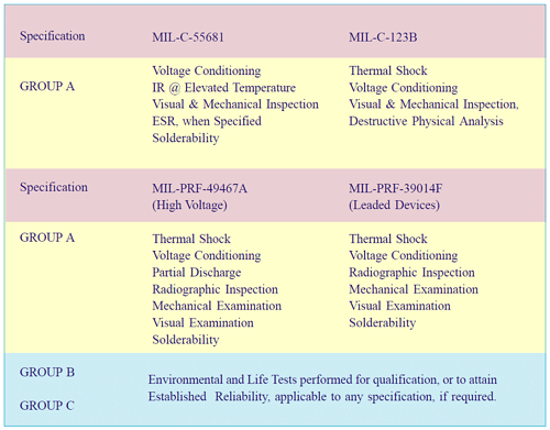

Table 1. High reliability test procedures

