

Interference Technology published an excellent article by Kenneth Wyatt on top reasons why electronic designs are failing EMI filtering testing.
The three top product failures I see constantly in my consulting practice are (1) radiated emissions, (2) radiated susceptibility, and (3) electrostatic discharge. After reviewing and testing hundreds of products over the years, I’ve come to the conclusion that products fail these tests for five common reasons (somewhat in order of incidence);
- PC Board Design—Poor layout and layer stack-up
- Cable Shield Termination and Pigtails—Cable shields are not terminated to enclosure or lack of common mode filtering for unshielded products, plus shield pigtails used
- Gaps in the Return Path—High frequency clocks or signals crossing gaps in the return path
- Power Distribution Design—Poor power distribution network (PDN) design
- Shielding Design—Apertures or slots in the shielded enclosure that are too long
1. PC BOARD DESIGN

To reduce EMI, we need to minimize the area of these loops. Undefined return paths often result in large current loops from source to load and back to source. These large current loops start to look like loop antennas, coupling noise currents to “antenna-like” structures, such as cables, in your product or system.
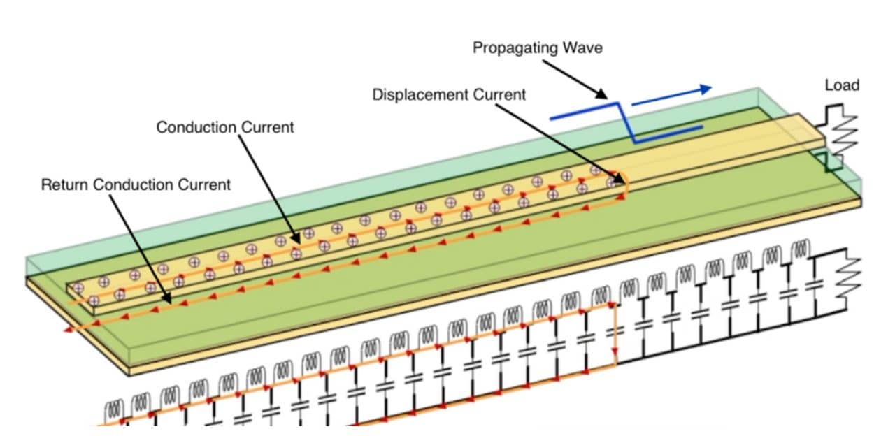
How Signals Move—At frequencies greater than about 50 to 100 kHz, digital signals start to propagate as electromagnetic waves in transmission lines. As shown in Figure 2, a high frequency signal propagates along a transmission line (circuit trace over return plane, for example), and the wave front induces a conduction current in the copper trace and back along the return plane. Of course, this conduction current cannot flow through the PC board dielectric, but the charge at the wave front repels a like charge on the return plane, which “appears” as if current is flowing. This is the same principle where capacitors appear to “pass” AC current, and Maxwell called this effect “displacement current”.

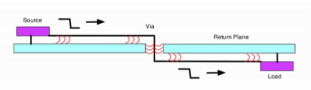
In order to satisfy both the circuit and field theory viewpoints, we now see the importance of adjacent power and power return planes, as well as adjacent signal and signal return planes. Signal or power routed referenced to a single plane will always have a defined return path back to the source. Figure 3 shows how the electromagnetic field stays within the dielectric on both sides of the return plane. The dielectric is not shown for clarity.

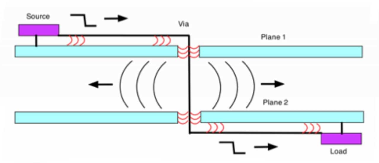
On the other hand, referring to Figure 4, if a signal passes through two reference planes, things get a lot trickier. If the two planes are the same potential (for example, both are return planes), then simple connecting vias may be added adjacent to the signal via. These will form a nice defined return path back to the source.

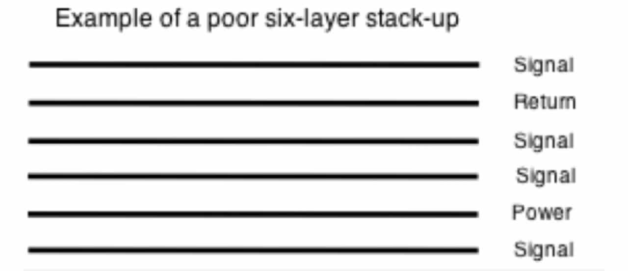
For example, let’s take a look at a poor (but very typical) board stack-up that I see often (Figure 5).

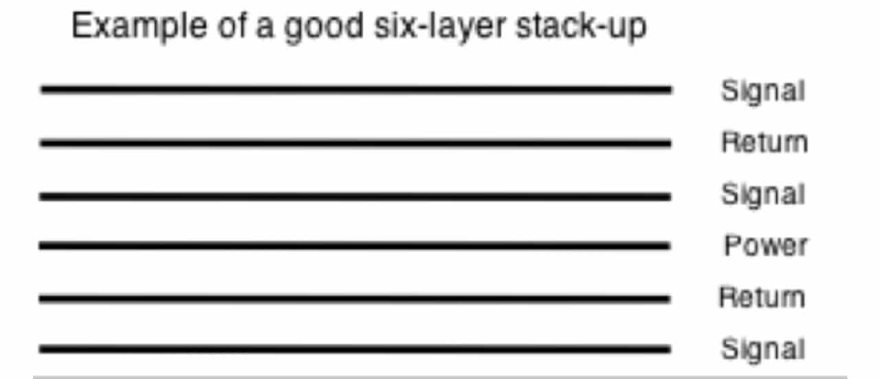
A better design is shown in Figure 6. Here, we lose one signal layer, but we see the power and power return planes are adjacent, while each signal layer has an adjacent signal (or power) return plane. It’s also a good idea to run multiple connecting vias between the two return planes in order to guarantee the lowest impedance path back to the source. The EMI performance will be significantly improved using this, or similar designs. In many cases, simply rearranging the stack-up is enough to pass emissions.

2. CABLE SHIELD TERMINATION
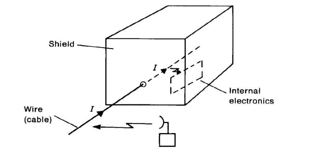
Cable Penetration—The number one issue I find when tracking down a radiated emissions problem is cable radiation. The reason cables radiate is that they penetrate a shielded enclosure without some sort of treatment – either bonding the cable shield to the metal enclosure or common mode filtering at the I/O or power connector (Figure 7 and 8). This occurs frequently, because most connectors are attached directly to the circuit board and are then poked through holes in the shield. Once the cable is plugged in, it is “penetrating the shield” and EMI is the usual result.


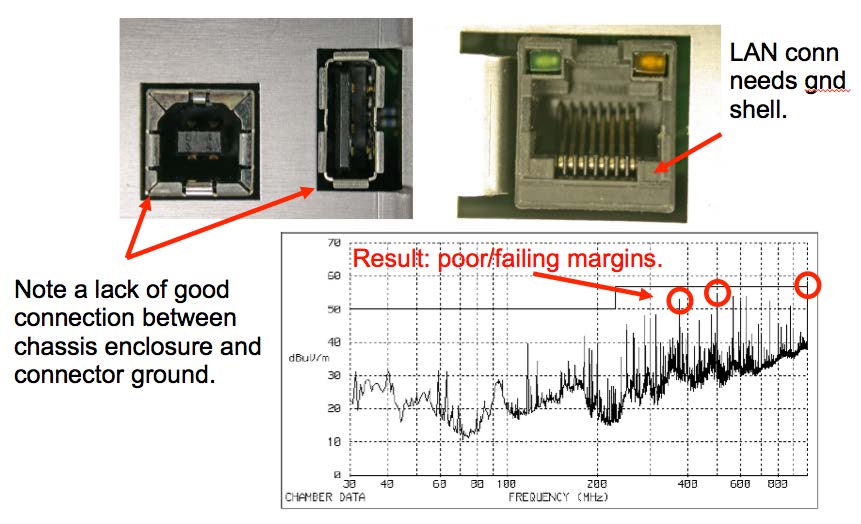
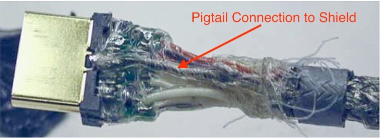
Cable Shield Terminations—Another potential issue is if the I/O cable uses a “pigtail” connection to the connector shell (Figure 9). Ideally, cable shields should be terminated in a 360-degree bond for lowest impedance. Pigtails degrade the cable shield effectiveness by introducing a relatively high impedance. For example, a 1-inch pigtail connection has 12 Ohms impedance at 100 MHz and gets worse the higher you go in frequency, thus defeating the cable shield.

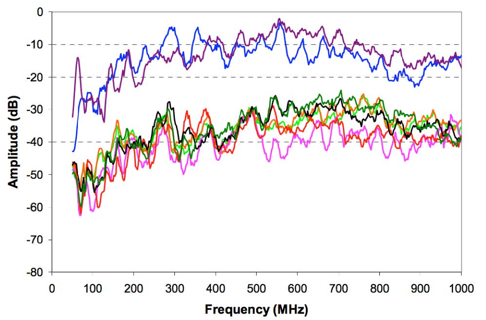
Here are the results in testing eight different brands of HDMI cable (Figure 10). Each was driven with a signal generator and measured in an EMI chamber while sweeping the frequency.

3. GAPS IN THE RETURN PLANE
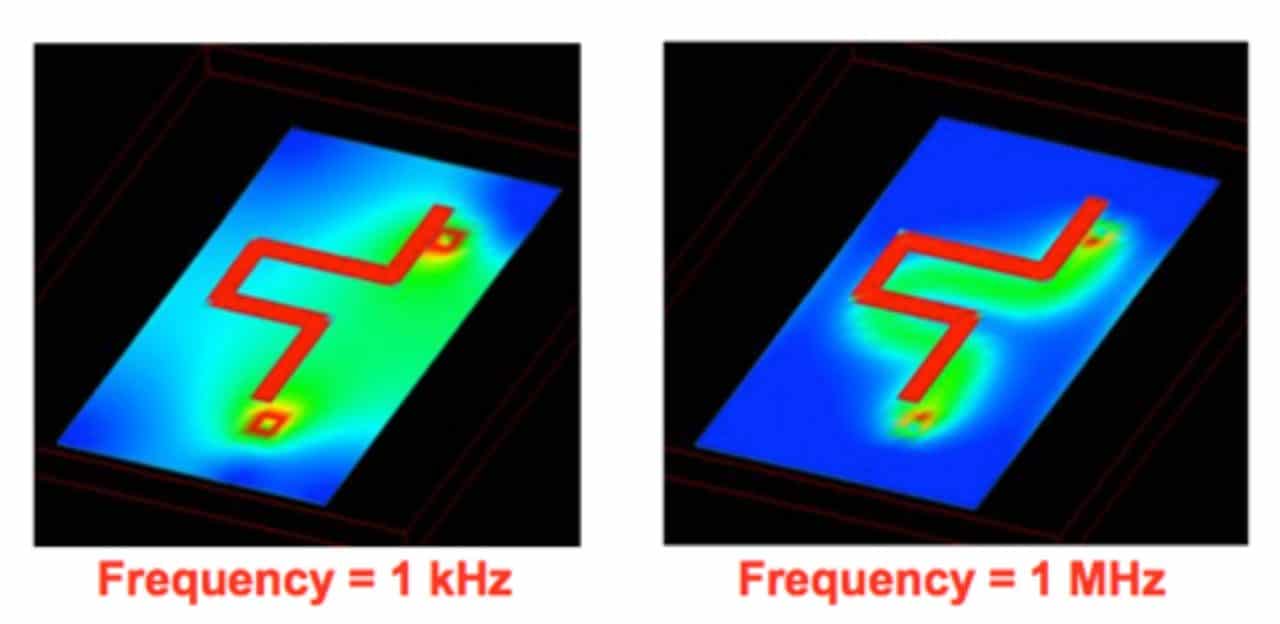
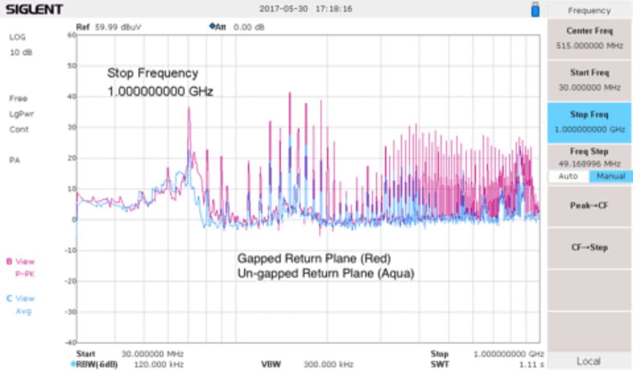
Breaks or gaps in the return path are major causes of radiated emissions, radiated susceptibility, and ESD failures. Let’s come back to the issue of a gap or slot in the return plane mentioned earlier and show an example of why it’s bad news for EMI. When the return path is interrupted, the conduction current is forced around the slot, or otherwise finds the nearest (lowest impedance) path back to the source. The electromagnetic field is forced out and the field will “leak” all over the board. I have an article and good demonstration video of this and how it affects common mode currents and ultimately, EMI. See Figure 11 and Reference 6. This would be a great demo to construct and show your own colleagues!

The difference between the gapped and un-gapped traces is shown in Figure 12. Note the harmonic currents are 10 to 15 dB higher for the gapped trace (in red). Failing to pay attention to the signal and power return paths is a major cause of radiated emissions failures.

4. POWER DISTRIBUTION NETWORK DESIGN
Power distribution network (PDN) design requires a low impedance (0.1 to 1.0 Ohms, typically) transmission line through at least 30 MHz. The purpose of a PDN is to transfer energy from the power source (often a voltage regulator module on the PC board) to the switching IC as fast as possible.
Capacitors, in the form of bulk, decoupling, and board capacitance, are used to store enough energy to overcome the tendency of the power rail voltage to decrease. Figure 13 shows a typical circuit model of a PDN with the power source on the left, supplying energy to the IC on the ight. In between, we have a series of energy storage capacitors and transmission lines (PC traces). Unfortunately, it takes significant time to transfer the required energy from the power source to the IC. It ha been shown that it takes about 600ps to transfer an amp of current across 1/16th inch of die bonds (Reference 10). That’s why it’s especially important to keep PDNs short and direct as possible.

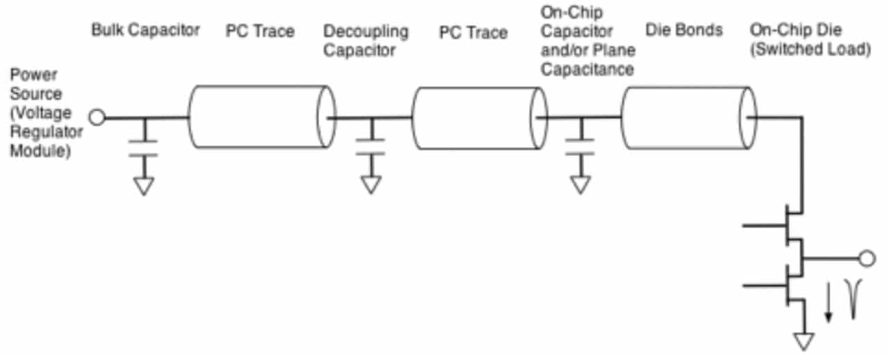
Ideally, the total energy demand will be met by the “on-chip” capacitors, if any, plus the energy stored in the power plane capacitance. However, these are seldom enough storage, so we depend a lot on nearby decoupling capacitors to supply the remaining energy demand. It is critical for the decoupling capacitors to have as little series inductance (in the form of internal inductance and trace inductance) as possible. The greater this series inductance, the harder it is to supply the required energy to the load and SSN results with related noise coupling throughout the PC board.
Assuming the decoupling and any built-in capacitance of the PC board can supply the energy needs, then the job of the bulk capacitor is to “recharge” the energy of the downstream capacitors in between switching transients. For the fastest recharge times, the PDN must be in the form of low impedance transmission lines.
The bulk capacitors 4.7 to 10 μF, typ.) are usually placed near the power input connector and the decoupling capacitors (1 to 10 nF, typ) nearest the noisiest switching devices to achieve the lowest series inductance, all decoupling capacitors should be mounted as close to the IC to be decoupled as possible and right over (or close to) the connecting vias. Multiple vias should be used for each end of the capacitor to further reduce series inductance. More on PDN design may be found in References 7, 8, and 9.
5. SHIELDING DESIGN
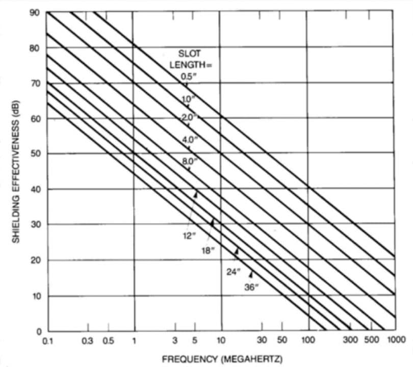
The two issues with shielded enclosures is getting all pieces well-bonded to each other and to allow power or I/O cable to penetrate it without causing leakage of common mode currents. Bonding between sheet metal may require EMI gaskets or other bonding techniques. Figure 14 shows a handy chart for determining the 20 dB attenuation of a given slot length. For example, if a product design requires at least a 20 dB shielding effectiveness, then the longest slot length can be just one-half inch.

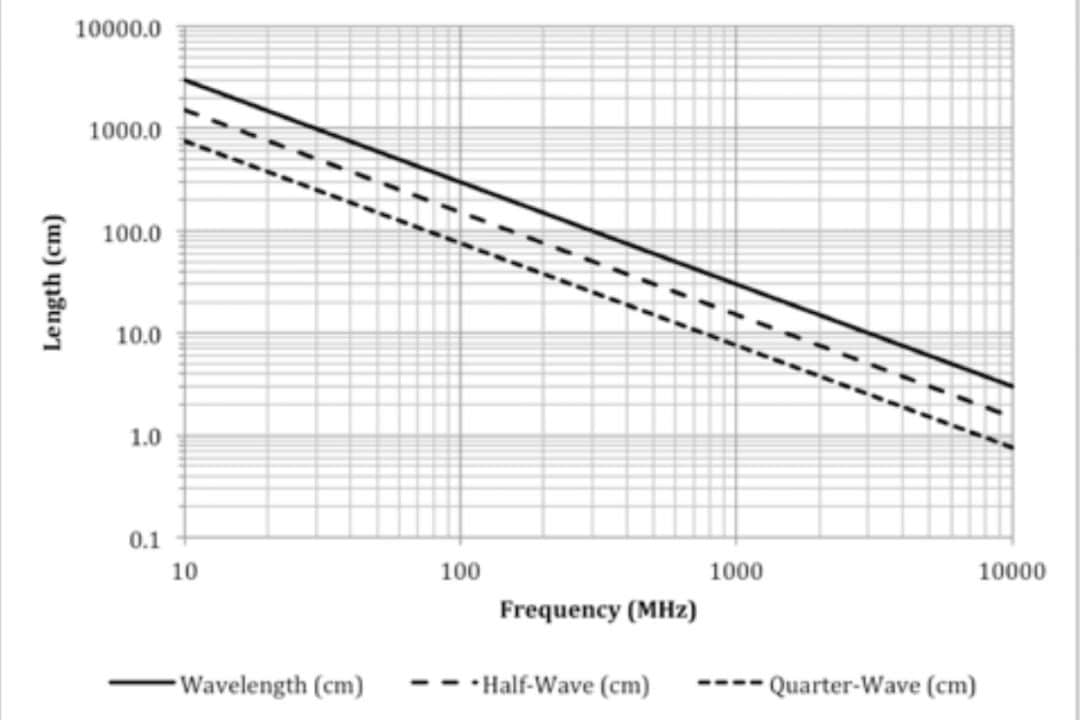
Slots or apertures in shielded enclosures become issues when the longest dimension approaches a half wavelength. Figure 15 is a chart of wavelength versus frequency. For example a 6-inch (15 cm) slot has a half wave resonance at 1000 MHz. Generally, ventilation holes should be patterns of round holes no more than 1/4-inch diameter. Patterns of slots may be used, but they should be no longer than 1/2-inch in order to preserve an adequate shielding effectiveness.

Reference 10 and 11 for more detail on shielding. Interference Technology also has a free downloadable 2016 EMI Shielding Guide with excellent information (Reference 12).
SUMMARY
Paying attention to these five product design faults will go a long way towards lowering the risk of EMI failure during formal compliance testing. Considering a proper EMC design early in project development will save tons of time and money in the end.
REFERENCES
- Bogatin, Signal Integrity – Simplified, Prentice-Hall, 2009.
- Morrison, Grounding and Shielding – Circuits and Interference, Wiley, 2016.
- Morrison, Digital Circuit Boards – Mach 1 GHz, Wiley, 2012.
Beeker, Effective PCB Design, https://www.nxp.com/files-static/ training_pdf/WBNR_PCBDESIGN.pdf
Bergey & Altland, EMI Shielding of Cable Assemblies, DesignCon 2008, http://www.magazines007.com/pdf/DC08_Dana_Bergey.pdf
Wyatt, Gaps in Return Planes – Bad News for EMI (with video demo), https://interferencetechnology.com/gaps-return-planes-bad-news-emi/
- Smith and Bogatin, Principles of Power Integrity for PDN Design, Prentice-Hall, 2017.
- Sandler, Power Integrity – Measuring, Optimizing, and Troubleshooting Power Related Parameters in Electronic Systems, McGraw Hill, 2014.
- Novak and Miller, Frequency-Domain Characterization of Power Distribution Networks, Artech House, 2007.
- Ott, Electromagnetic Compatibility Engineering, Wiley, 2009
- André and Wyatt, EMI Troubleshooting Cookbook for Product Designers, SciTech, 2014.
- Interference Technology’s 2016 EMI Shielding Guide, http://learn. interferencetechnology.com/2016-emi-shielding-guide/
About the Author
Kenneth Wyatt is principal consultant of Wyatt Technical Services LLC and served as the senior technical editor for Interference Technology Magazine from 2016 to 2018. He has worked in the field of EMC engineering for over 30 years and specializes in product design for EMC compliance, EMI troubleshooting and pre-compliance testing. He is a co-author of the popular EMC Pocket Guide and RFI Radio Frequency Interference Pocket Guide. He also coauthored the book with Patrick André, EMI Troubleshooting Cookbook for Product Designers, with forward by Henry Ott. He is widely published and speaks internationally. Kenneth is a senior member of the IEEE and a long time member of the EMC Society. Check out his web site for more technical information, training schedules, and contact information: http://www.emc-seminars.com.
Read the full paper on the link below

