
Source: Alter Technology article
by Francisco Javier Aparicio Rebollo. Thermoreflectance Thermal Imaging is a powerful tool as a thermal characterization technique for microelectronics and discrete components.
The temperature gradient in integrated circuits
Submicrometric-nanometric objects nowadays present in the design of integrated circuits induce singular heat transport phenomena leading to the formation of hot-spots or strong temperature gradients at specific focal points, which compromises the suitable operation and reliability of microelectronic systems and can potentially decrease the lifetime. The typical length of such singularities can reach the micro and submicronic scale. Hence temperature gradient over such systems has to characterized by advanced thermography instruments with high spatial resolution.
Why TTI?
Thermoreflectance Thermal Imaging (TTI) is a microscopy technique that provides temperature gradient contrast by analyzing the optical reflectance of the inspected surfaces. Amongst others, TTI is employed to:
- 2D thermal mapping.
- Failure analyses and testing of microelectronic devices
- The visualization of high-speed thermal transients
- to study the implementation of innovative materials.
Main characteristics and advantages of the technique are:
- Non-contact character.
- High spatial resolution (micron and submicrometric), limited by the diffraction limit.
- Temporal resolutions ~ 100µs.
- Wide range of temperature detection.
How does it work?
TTI exploits of the linear effect that the temperature has on the surface reflectivity (Eq. 1).
As illustrated in the figure, when the sample has irradiated the intensity of the reflected beam depends on the local temperature of the irradiated zone. Thus hot spots, as the red square in the figure, increase the intensity of the reflected beam. Therefore, the accurate analysis of the reflected beam at the selected areas provides a thermal map of the device surface.

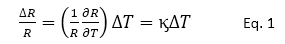
Change of the intensity (reflectivity) due to the temperature
Practical Applications:
This mapping technique provides useful information about the power dissipation profile and hot spots related to the design of microelectronics devices. Besides it is also used for the early detection of design, manufacturing or material defects in microelectronics systems.
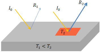
Appl Phys., 2006; 39: 4153-4166; Optical and thermal image of the heating resistor
The figure illustrates the compare an optical and a thermal image of a five broad polysilicon resistive stripes (heaters). Thanks to this technique it is possible to obtain the temperature map placed at the right of the image. This image results from an accumulation of over 200 heating periods and a total acquisition time of 1 min in practice.
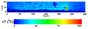
To illustrate the high spatial resolution and the detection of micrometric hot spots the following image also shows the thermal analysis of high power semiconductor laser bars. In this case, it is clearly observed a micrometric hot spot at the face of one emitter (x = 225µm). This permitted the early detection of the ongoing mirror degradation, which eventually leads to catastrophic optical mirror damage failure.
Appl Phys., 2018; 51: 013001
Thermal imaging of an emitter laser bar
The spatial and temperature resolutions and sensitivity reached by thermoreflectance techniques are excellent, however, the accuracy of the absolute temperature readings is more difficult to evaluate due to the lack of comparable thermal techniques with submicrometric spatial resolution. Therefore, major applications of the technique on the microelectronics field involves analyzing the relative temperature gradients on the surface devices and similar studies such as thermal mapping applications, thermal transport studies, and hot spots analyses.
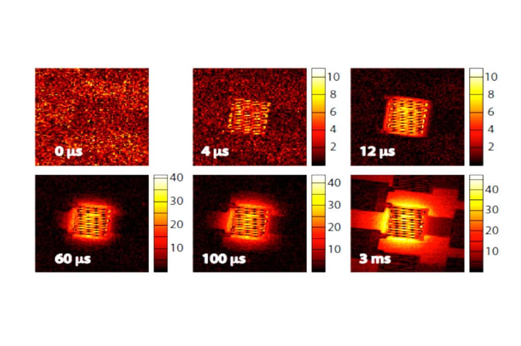
On the other hand, thanks to the high time resolution, ITT is also used for transient thermal imaging in switching devices or other systems under pulsed operation. This character is normally used to identify buried defects or help to extract the thermal resistance/capacitance network in the device, surrounding regions in the substrate and the package.
Time domain thermoreflectance imaging of a gold heater
The figure shows quick heat diffusion in the device metal on short and long time scale thermal imaging of a 100 micron integrated gold heater using pulsed boxcar averaging. The figure also illustrates how the technique is used to study the transitory heat transmission from the sample to other adjacent components.

