
Source: ALD Analogue Linear Devices article
By Paul Pickering, ALD
Supercapacitors are unique because they can work in conjunction with or as an alternative to batteries in applications needing many rapid charge/discharge cycles and are popular in applications such as short-term energy storage, regenerative braking, and static RAM memory backup. But balancing a supercapacitor in a design involves more than connecting a few wires. When a supercapacitor has an operating voltage of 2.5V – 2.7V, most applications use an array of devices connected in series for higher voltage.
Many supercapacitors have a leakage current which varies based on numerous factors, including:
- Initial leakage value
- Leakage variation with charging voltage, charging current and temperature
- Operating temperature range
- Chemistry, Material, and Construction
- Aging
In a cell, differences in leakage currents between individual supercapacitors result in changes in voltages across them over time; this can cause reduced lifespan and eventual failure since exceeding the maximum voltage on a supercapacitor can lead to cell failure.
Preventing this imbalance requires a balancing circuit that keeps the voltage across each supercapacitor within limits by automatically correcting the effects of changing leakage currents, all with minimal added leakage current or power consumption.
For the module designer, this represents an additional layer of complexity. A simple resistor-based design dissipates power and doesn’t respond to aging and temperature variations; an opamp-based design has higher performance, but is complicated, also wastes power and consumes excessive board space. Developing a solution also requires layout expertise and analog or power design skills; the result may be added development time or even make the problem worse and add unwanted leakage of its own.
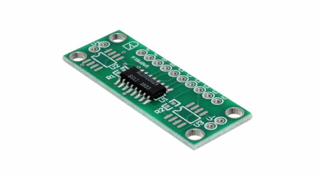
Overview of a new Printed Circuit Board
A new printed circuit board (PCB) offers a “plug and play solution” by combining all of the circuitry required to accomplish these tasks for any size supercaps. Figure 1 shows the board, which is designed to be used in conjunction with precision MOSFET arrays.
Each board measures only 0.6” x 1.6” and when fully populated can balance up to four supercapacitors connected in series; in addition to the unpopulated, populated boards
are available with different combinations of MOSFETS to reach required voltages. For larger arrays, any number of boards can be connected in series, subject only to a maximum voltage per board of 15V.


Figure 1 left: four supercapacitors plus external components courtesy of Advanced Linear Devices (ALD).
The board can accommodate supercapacitors from 0.1F to 3000F and beyond. The average additional power dissipation due to the use of the boards is zero, which makes this method of supercapacitor balancing very energy-efficient. It is especially suited for low loss energy harvesting and long life battery-operated applications.
Figure 2 shows the schematic of the board used with four supercapacitors C1 – C4. The MOSFET is an array of four identical chips; that contains two devices in an identical configuration. Depending on the board selected, each supercapacitor can have a single MOSFET, or two devices in parallel, connected across it. Connecting two devices in parallel gives an equivalent MOSFET with twice the output current and twice the sensitivity to voltage change.
The “XX” in both part numbers denotes the voltage across the MOSFET that corresponds to a leakage current of 1uA at 25°C, as discussed in the next section.
Each MOSFET is rated for a reverse bias diode current of up to 80 mA maximum. Any reverse bias condition as a result of changing supercapacitor voltages, especially during fast supercapacitor discharge, could lead to some internal nodes becoming reverse biased with surge current in excess of this limit.
The board has TO277 pads for adding external Schottky rectifiers (power diodes) to clamp such current transients.
An optional resistor can also be connected across each pair of supercapacitors. Normally this is left open, but if those two supercapacitor locations are unpopulated a zero-ohm jumper in the corresponding location should be installed.


Figure 2: schematic of a fully-populated board with three MOSFET arrays. The design ensures that the voltage across each supercap (VA – VB, for example) does not exceed the maximum allowed value. Courtesy of Advanced Linear Devices
Circuit Operation
How does the circuit automatically balance leakage? A MOSFET can be considered as a three-terminal voltage-controlled resistor over a limited operating range, with the “on” resistance RDS(ON) an exponential function of the input voltage VGS. When the gate and drain are connected, VDS is also equal to VGS, and called the threshold voltage Vt. Figure 3 shows the data for the quad MOSFET array.


Figure 3: The chip relative ON resistance vs. input voltage courtesy of ALD .
The “XX” in the ALD part numbers denotes the threshold voltage Vt that gives an output current IOUT of 1μA at 25°C. For example, the ALD810025 quad array has Vt = 2.5V, so IOUT = 1μA at 2.5V and 25°C. This corresponds to an RDS(ON) of 2.5MΩ. Table 1 shows the change in IOUT as Vt varies.
Output Current
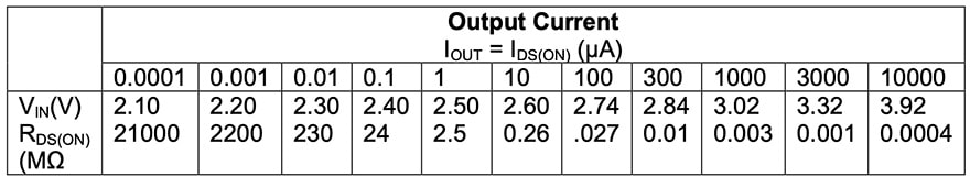

Table 1: Equivalent ON resistance at different input voltages and output currents for the ALD810025 at TA = 25°C.
When a MOSFET is connected across a supercapacitor in an array, the exponential relationship between Vt and RDS(ON) means that any small increase in the supercapacitor voltage caused by leakage current from another supercapacitor will cause a large decrease in the RDS(ON) of that MOSFET. This will increase IDS(ON) and reduce the voltage. As the voltage decreases, IDS(ON) will also decrease.
Depending on the PCB part number selected, each supercapacitor can have a single MOSFET or two devices in parallel connected across it. Connecting two devices in parallel gives an equivalent MOSFET with twice the output current and twice the sensitivity to voltage change.
The leakage current balancing mechanism is fully automatic and works for supercapacitor arrays with different leakage current profiles. In a stack with many supercapacitors in series, multiple MOSFET arrays function to balance the various leakage currents.
For example, if leakage current IC1 is greater than IC2 in the four-capacitor array in figure 2, then both M1s (in U1 and U2) are turned off and the M2 pair becomes the active circuit element to balance C1, the supercapacitor with the greatest leakage.
Without the auto-balancing circuit, the voltage across C2 can keep rising until it destroys the part. The MOSFET balancing solution contributes virtually no additional current drain and adjusts for temperature, time, and other environmental changes that may contribute to out-of-balance conditions.
When an MOSFET is connected across a supercapacitor in an array, any increase in the supercapacitor voltage caused by leakage current from another supercap will cause a decrease in the RDS(ON) of that MOSFET. This will increase IDS(ON) and reduce the voltage. As the voltage decreases, IDS(ON) will also decrease. The leakage current balancing is fully automatic and works for a variety of supercapacitors, each with a different leakage current characteristic profile.
The MOSFET balancing solution contributes virtually no additional current drain and adjusts for temperature, time, and other environmental changes that may contribute to out-of-balance conditions. In a stack with many supercapacitors in series, multiple SAB MOSFET arrays function to balance the various leakage currents. For example, if leakage current IC1 is greater than IC2 in the four-capacitor array in figure 2, then both M1s (in U1 and U2) are turned off and the M2 pair becomes the active circuit element to balance C1, the supercapacitor with the greatest leakage.
Without the auto-balancing circuit, the voltage across C2 (VB – VC) can keep rising until it destroys C2 with overvoltage.
By providing a plug-and-play solution to the problem of balancing leakage currents in supercapacitors, the new PCB saves both time and effort for designers who must integrate them into their modules.

