
Source: InCompliance article
by Arturo Mediano.
When designing EMI filters, how and where the filter is installed is critical to obtain the desired insertion losses. Usually, the effect of a wrong location or installation is not considered in the design of the filter and surprises appear.
A few weeks ago I was working on a product of a company failing in conducted emissions. The product was powered from 240V 50Hz (Europe) mains network consuming 10A and a custom filter was included in the design to try to pass the regulations for conducted emissions in the 9kHz-30MHz range.
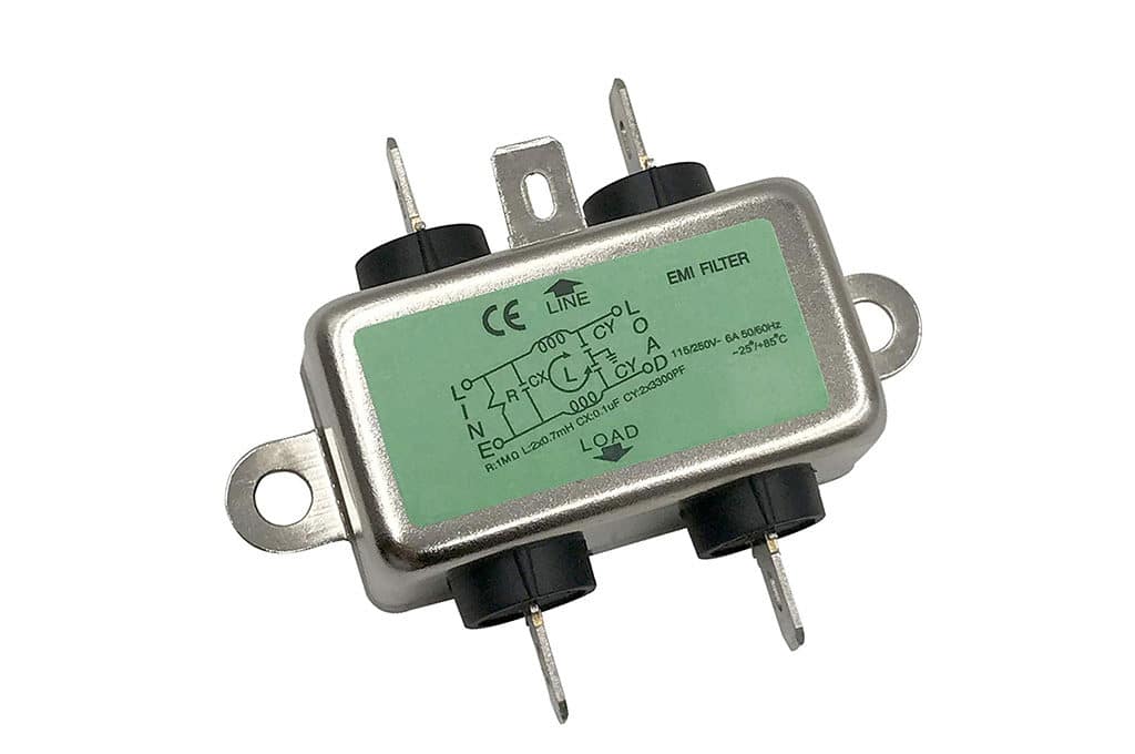
The schematic of the filter used in this product is included in Figure 1. The filter was composed of two 100nF X2 capacitors, one 470uH common mode choke, and two 4.7nF capacitors.


But, the results obtained in the EMC test house by the company were really bad (>20dB) compared with the expected results from theory and simulation in the range from 1MHz to 10MHz.
When a filter is not working as expected I usually check some typical points:
- What terminal impedances were used in the design? Many designers use 50ohms because this is a good value for testing the filter with common RF instruments. But, if your product does not present 50ohms impedance, surely the behavior of the filter will be different [1].
- Are the inductors used in the filter being saturated? This is more typical in differential mode filters but sometimes leakage or external magnetic fields can saturate common mode chokes.
- Were the parasitics of components (especially self-resonant frequencies) included in the design process? Usually, the frequencies higher than 1MHz are compromised especially if big inductors and capacitors are needed.
- Where is the filter installed? A good location for the filter is far from noisy areas. As, for example, floating power electronic heat sinks. This is critical if the filter is non-shielded.
In my analysis, I was able to identify that none of the previous effects were the origin of the problem so I went to check how the filter was wired and I found that the input and the output of the filter were really close to each other. This is a dangerous situation, especially for the high frequency range.
I have partially reproduced the effect so you can understand the idea (exact identification and pictures of the system remain confidential).
Consider, for example, that you have a filter shielded as the one in Figure 2. Note that, in theory, we will be expecting a low pass differential filtering response.


Now, consider Figure 3 where the filter is installed with input and output cables close to each other.


Now, the position of cables creates some kind of coupling between the input and the output of the filter. This coupling can be capacitive (electric field) and inductive (magnetic field) so the theoretical low pass filter response is “short-circuited” and the signals can go from the input to the output easily (especially in the high frequency range). In Figures 2 and 3, I am not considering the parasitic effects of components.
To check the installation of the filter in our product, I used my Bode 100 network analyzer with the product OFF. The results are included in Figure 4.


Note the response at low frequencies (<600kHz) is not affected by the parasitic IO feedback. But, it is degraded up to 30dB in the 1-10MHz frequency range when IO feedback is present similar to Figure 3.
It is interesting to note from our measurements the peak in the response at 361kHz (cursor 1, green). This is a very dangerous situation if the peak goes over 0dB and not related with the IO feedback (topic for a future article).
Note, too, how the low pass response in the filter is dominated by parasitic in components at frequencies higher than 2.5MHz (cursor 2, orange).
My final advice: when doing the layout for a filter in both wired or PCB formats, BE CAREFUL with the I/O feedback. Try to route the lines correctly to minimize the parasitic feedback that degrades the filter response in high frequencies.
References
- A. Mediano, “S Parameters and EMI Filter Response,” pp. 15-17, In Compliance Magazine, August 2018.

