
source: signal integrity journal article
January 2, 2018, Anto Davis and Steve Sandler. A negative coupling coefficient to optimize capacitor placement may not always lead to lower impedance.
It is well known that the mounting loop of a capacitor owns the major share in parasitic inductance [1]. A practical capacitor when mounted in a printed circuit board has parasitic inductance (L) associated with it. Its equivalent circuit is a series RLC circuit where R represents the loss associated with the capacitor (C). It has a self (series) resonant frequency given by![]()

A mounting loop is formed by the two vias connecting a capacitor to the power-ground planes. A small form factor capacitor reduces this area and helps to minimize the parasitic inductance. Closer power-ground planes reduce the plane spreading inductance.
Geometry for Negative Coupling Coefficient
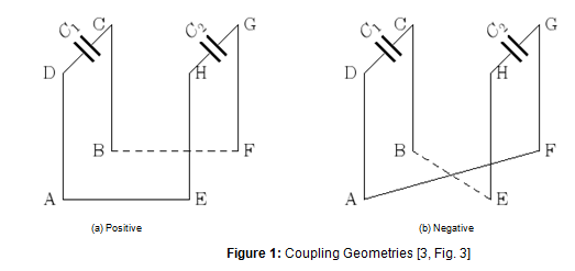
With two capacitors in parallel, we can generate a negative coupling coefficient to reduce the parasitic inductance. This is shown in Figure 1. Points A and E are on the same plane and points B and F are on the same plane. Assume that the planes are power and ground separated by thin dielectric of thickness (2-3 mils).
Figure 1(b) shows the geometrical connection for negative coupling coefficient (M and k are negative). When power and ground planes are present, this geometry can be achieved by changing via locations; B and E are on the same plane and A and F are on the same plane.
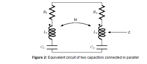
Figure 2 shows the equivalent circuit diagram of two capacitors in parallel. Writing equations for it,


1. Identical Capacitors
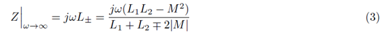
For large values of w, the Eq. 2 becomes the classic equation of coupled parallel inductors.

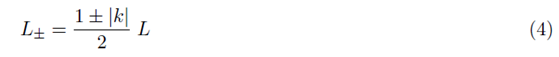
where + and – signs indicate positive and negative couplings. For equal loop areas (L1 = L2 = L), inductance is given by,

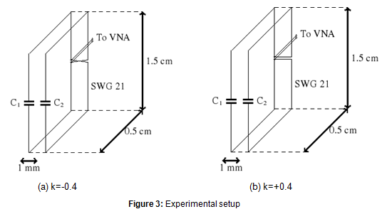
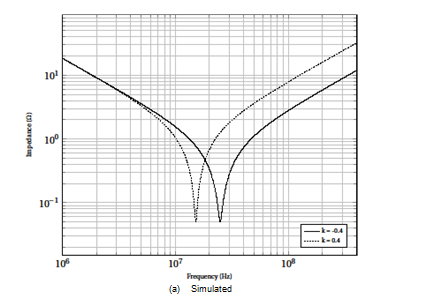
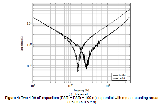
Experiments are conducted with two ceramic disc type capacitors of values C1 = C2 = 4.7 nF. Measurement with a capacitor meter gives their values as 4.30 nF. The leads are cut and made with insulated copper wire of SWG 21 (diameter = 0.813 mm). Leads make a loop of area 1.5 cm _ 0.5 cm. The measurement device is Rohde & Schwarz vector network analyzer (VNA). The scattering parameters measured are converted to impedance values. VNA is set with the following values: Resolution band width (RBW) = 10 Hz; number of points = 1000; and power = -15 dBm. Two loops are kept at a distance of 1 mm (edge to edge). The coupling coefficient between the loops (k = M/L) is calculated to be 0.4 where L is 17.6 nH and M is 6.97 nH [2]. Simulation and experimental results are shown in Fig. 4(a) and Fig. 4(b) respectively. At 100 MHz, inductance is 2.5 times (8 dB) lesser than that for positive coupling case.


No surprises until here. How about the case where the two capacitor values are different?
Non-identical Capacitors
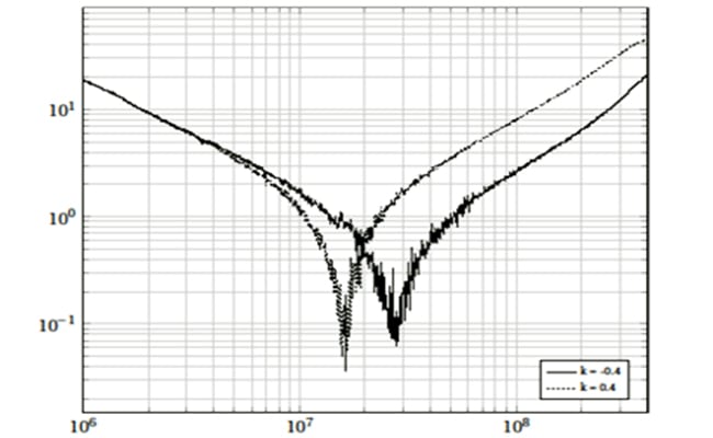
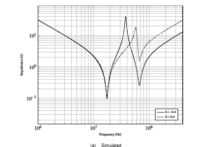
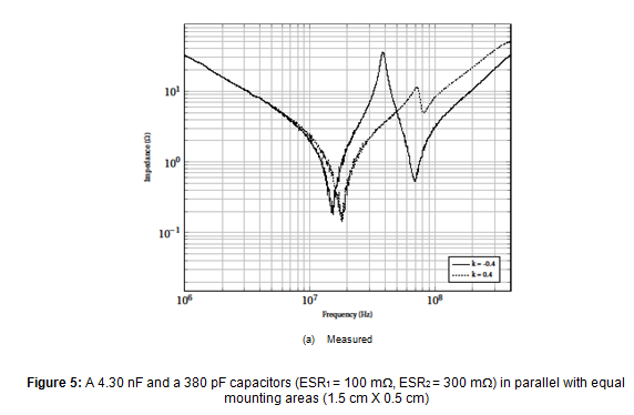
When the capacitor values are different, the parallel combination produces antiresonance peaks as shown in Figure 5. The anti-resonance peak is lower for the positively coupled case. It is assumed that the capacitors have nearly equal mounting inductance, and their sizes are comparable. Experiments are conducted for the same values of the previous experiment, except that one capacitor is changed to 390 pF. A measurement with capacitance meter gives 380 pF for this capacitor. Experimental results (Figure 5(b)) shows that the antiresonance peak is lower for positively coupled case by 3.2 times. When both the capacitors become inductive, the equivalent inductance is lower for negative coupling case.


Summary
A negative coupling coefficient produces a larger anti-resonant peak compared to a positive coupling coefficient, even though the equivalent inductance is lower. Multiple anti-resonant peaks are capable of generating rogue waves [7, 8], and suppressing them are becoming more and more important. For low noise circuits, power distribution network (PDN) resonance is an important design issue, and should be suppressed!
How about the tolerance of two identical ceramic capacitors connected in parallel? `It depends’ on the type of capacitors that determines the capacitance variations. Plotting eq. (2) with worst-case values will give the answer. Authors leave this to the curious reader to explore!
A. K. Davis (ECE, GeorgiaTech, Atlanta, USA) & S. M. Sandler (Picotest, Phoenix, AZ 85085, USA)
2. References
[1] Roy, T., Smith, L., and Prymak, J.: `ESR and ESL of ceramic capacitor applied to decoupling applications’, IEEE 7th Top. Meet. Elect. Perform. Electron. Packag., 1998, pp. 213-216.
[2] Paul, C. R.: `Effectiveness of multiple decoupling capacitors’, IEEE Trans. Electromagn. Compat., 1992, 34, (2), pp. 130-133.
[3] Davis, A.K.: `Effect of magnetic coupling between the mounting loops of two parallel capacitors on antiresonance’, IET Sci. Meas. Tech., 2016, 10, (8), pp. 889-899.
[4] Davis, A.K., and Gunasekaran, M.K.: `Microprocessor-conducted noise reduction with switched supercapacitors’, Electron. Letters, 2014, 51, (1), pp. 92-94.
[5] Novak, I., Pannala, S., and Miller, J. R.: `Overview of some options to create low-Q controlled-ESR bypass capacitors’, IEEE 13th Top. Meet. Elect. Perform. Electron. Packag., 2004, pp. 55-58.
[6] Davis, A.K.: `Effect of a magnetically coupled resistive loop on antiresonance’, Electron. Letters, 2016, 52, (13), pp. 1162 – 1164.
[7] Steve Sandler: `Target impedance based solutions for PDN may not provide realis-tic assessment’, available https://www.edn.com/design/test-and-measurement/4413192/Target-impedance-based-solutions-for-PDN-may-not-provide-a-realistic-assessment
[8] Eric Bogatin, Istvan Novak, Steve Sandler, Larry Smith, Brad Brim, and Steve Weir: `Target Impedance and Rogue Waves’, available http://www.electrical-integrity.com/Paper_download_files/DC16_TargetImpedanceRogueWaves-panel.pdf

