

The high-κ dielectric materials are commonly used in microelectronic components due to technological necessity of increasing the permittivity of dielectric layers. The thickness of the layer is crucial parameter of this technology because it has significant influence on the dielectric properties, capacitance density, leakage current density-voltage (J-V), and capacitance density-voltage (C-V) characteristics.
The paper was presented by Jaromir Hubalek, Brno University of Technology, Czech Republic at the 3rd PCNS 7-10th September 2021, Milano, Italy as paper No.5.2.
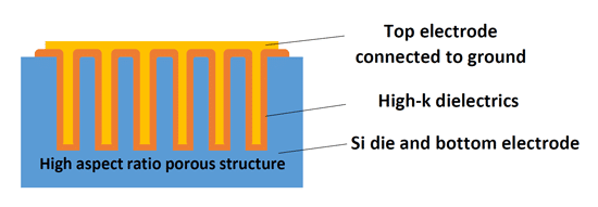
Among metal oxide compounds, HfO2 and Al2O3 have been widely studied due to their good thermodynamic stability in contact with silicon. The devices have been fabricated by ALD processes on Si wafer. Properties of HfO2/Al2O3-based dielectric as on-chip MIS capacitors were studied. The capacitance density, C-V and impedance characteristics, and leakage current were measured. The equivalent dielectric constant, capacitance density, breakdown voltage and leakage current are studied on stacks (HfO2/Al2O3) in ration of 1:1. The experimental results indicate very good leakage current and good breakdown voltage. The trenches with aspect ratio 1:28 were developed to form 3D structure for future increasing capacitance density on square centimetre. Top electrode metallization using several different techniques to fill in the trenches was also studied.
INTRODUCTION
The high-κ dielectric materials are widely used in the microelectronics due to downscaling of device sizes. An on-chip capacitors are integrated also as component in analogue integrated circuits. Using capacitors for energy storage is more intensive in last decade [1], [2]. High-κ dielectric nanolaminates are being investigated in memory storage capacitors and charge storage. Choosing the right composition of dielectric materials, thicknesses and structures are crucial factors resulting in different properties of nanolaminate structures such as capacitance density, leakage current density-voltage, capacitance density-voltage. Thermodynamic stability of HfO2 and Al2O3 with silicon is reason of investigation of these materials. Al2O3 shows highest band gap but relatively low dielectric constant [3] which can be increased by adding HfO2 with relatively high dielectric constant, but also increased leakage currents of capacitor. Optimizing the composition of stacks of these materials is key element to enhance properties of capacitors. Stack consisting of one layer of Al2O3 a HfO2 are commonly used and are well described [4], [5], [6].
In this work we compare properties of high-κ dielectric with the stacks composition based on two materials HfO2:Al2O3. with Al2O3 as a top layer. Al2O3 serves as passivation layer to avoid deterioration of HfO2 properties and improving the metal/dielectric interface. Furthermore, the performance of nanolaminate capacitors are compared with each other showing that the more layers outperform the lower number of layers. Higher number of layers showing lower leakage currents and higher dielectric constant. Improvement of capacitance properties of HfO2-Al2O3 nanolayers used as on-chip MIS capacitors fabricated by plasma-assisted ALD is demonstrated.
EXPERIMENTAL
Investigation of the electrical properties, dielectric constant, breakdown voltage and leakage current density of stacked structures composed of HfO2 and Al2O3 is aimed in this study. Investigated stacks composing of alternating layers of Al2O3 and HfO2 are deposited by atomic layer deposition (ALD) on n-type silicon wafer with 1 nm of native SiO2. Total thickness of the dielectric films is the same and equal to 12 nm.
Silicon substrates were cleaned using Radio Corporation of America (RCA) cleaning method. Next step was usage of 5% HF aqueous solution eliminating native oxides on the surface of substrates but still 1 nm of oxide could grow before closing the wafer to ALD chamber. HfO2/Al2O3 layers were deposited by plasma assisted ALD technique at 250 °C and 300 W. Precursors used for deposition were Tetrakis (ethylmethylamino) hafnium (TEMAHf) (Hf[N(CH3)(C2H5)]4) and trimethyl aluminium (TMA) [Al(CH3)3] with O2 plasma as reactant. Deposition speed was 0.9 Å/cycle for Al2O3 and 1Å/cycle for HfO2, respectively. All layers of the sample were deposited continuously without breaking vacuum.
Lithographical lift-off process was involved to create top electrode using positive photoresist AZ1518 (Microchemicals GmbH) and mask aligner SUSS MA08 (Suss Microtec) and bottom electrode was metalized with sputtering by 200 nm of aluminium layer representing ohmic contact and reducing Schottky contact.
For J-V characterisation, Cascade Microtech MPS 150s probe station and Keithley SMU 2636B Sourcemeter were used. C-V characteristics were measured using Keitlhley 4200A-SCS parameter analyzer and shielded Semi-automated 4-probe system Cascade Microtech SUMMIT 12000. Trenches were fabricated as a ~10 × 10 mm silicon chips on 4‑inch Si wafer <100> (Siegert Wafer, Germany) a ~525 μm thick. AZ 5214E high resolution positive photoresist was used as a DRIE process protective mask. The Oxford Instruments Plasma Technology (UK) PlasmaPro 100 DRIE machine with 3 kW, 13.56 MHz Inductive Coupled Plasma (ICP) source was used for fabrication and process optimization. Ion beam assisted deposition (IBAD, Bestec, DE) and Metal Organic Chemical Vapour Deposition (MOCVD, SVCS Process Innovation, CZ) were tested for top electrode metallization.
DIELECTRIC PROPERTIES STUDY
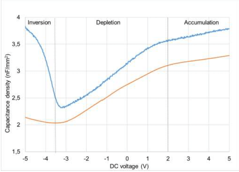
The C-V measurements were done due to MIS structure of the capacitor under test. In Fig.1 C-V measurements are shown at low frequency (10 kHz) and high frequency (1 MHz) for all samples showing lowest and highest capacitance. Due to n-type substrate the inversion region is obtained at negative voltage (below -3V). Increasing of DC bias voltage led to capacitance increase till accumulation regime (above 2 V) were the slope was already smaller. The shape of C-V curves is related to the amount of charged defects at interface between insulator and semiconductor. Above 0 V in depletion region and for accumulation one, the capacitance is increasing with number of layers for both measurements 10 kHz and 1 MHz, respectively. In depletion part, the leakage currents can be found slightly improved by number of layers.

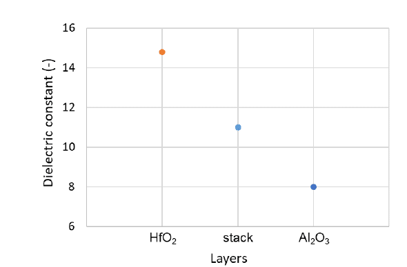
The dielectric constant of the samples was calculated from capacitance value in depletion region due to low leakage. In Fig. 2. It shows that dielectric constant of the stack lay in the middle of single layers (Al2O3 and HfO2). Calculation was done from depletion at 0 V in C-V characteristic using equation C/A = κε0/d where C, A, d, ε0 are capacitance, area of capacitor (diameter is 250 μm), thickness of dielectric layers and permittivity of free space. Thickness was estimated to 12 nm including 1 nm of native SiO2 that was the same in all samples. Therefore, the contribution of the SiO2 layer is the same in all samples and regarding to its permittivity it is smaller than in case of stacks.
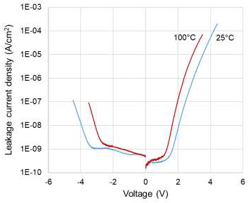
The leakage currents of nanolayered on-chip capacitors were evaluated from J-V curves that have been measured at room temperature (25 °C) and at 100 °C. As shown in Fig. 3. there are two regions in these characteristics. One is in the depletion region where leakage currents are around 10-9 A/cm2 and increases very slowly. Second is in the accumulation above 2 V and inversion region below -3 V where increasing of leakage start to be controlled by the electron emission field causing cold electron tunnelling. In the depletion region leakage currents are slightly decreasing with number of stacks at both temperatures. In accumulation part (> 2 V) more layers are showing higher leakage currents at both temperatures.
At low temperatures, the leakage currents exhibit weak dependence on temperature. The effect of cold electron tunnelling was shifted from 2V to 1.5 V while at negative part from -3.5 V to -2.5 V as temperature changed from 25°C to 100 °C. Rapid increase of the leakage currents due to cold electron tunnelling above 2 V or below -3.5 V can be depressed by optimisation of ALD process because the tunnelling currents depend on stoichiometry of the dielectric material.


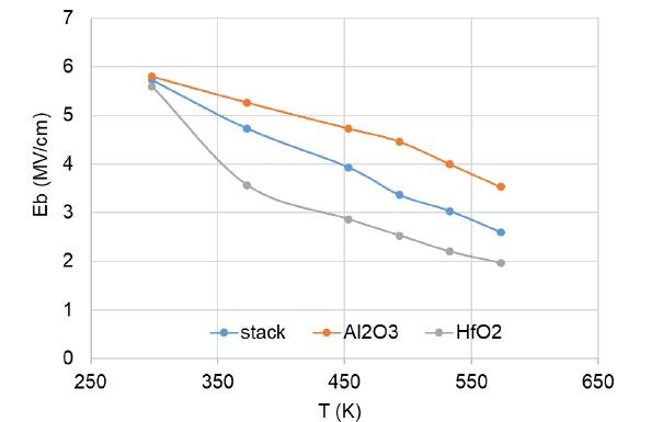
The typical breakdown voltage of Al2O3 dielectric layer is 5 MV/cm [7 and of HfO2 nanolaminates in range of 5-9 MV/cm [8] for 10 nm thickness at room temperature. For our films we have obtained breakdown energy about 5.8 MV/cm for all samples (Fig. 4). Nanolaminates thinner then 10 nm are susceptible to breakdown [9].
3D structure development
When on-chip capacitors has to be fabricated with sufficient capacitance density, the tranches have to be created in bulk of the die. The Deep Reactive Ion Etching (DRIE) cryogenic process had to be optimized for 4” wafers [8]. We optimized CCP power in order to prevent a reduction of selectivity, under-etching, black silicon formation and complete process stopping when wrong parameters. We also tuned oxygen concentration in plasma to prevent black silicon formation and to obtain sufficiently thick passivation layer on the trenches walls to prevent etching trough the walls between individual trenches. The aspect ratio of 1:28 was finally achieved on a whole wafer in a two steps DRIE process (see Fig. 5).

The MOCVD metallization was performed using several precursors. However, the process was not well performed due to experimental equipment in use. Side wall covering was very poor The second technique, which was used, Ion Beam assisted Deposition (IBAD) was very promising. 3D structures were sputtered by aluminum film with top surface thickness ~1 μm. The sidewall thickness of aluminum layer was ten times thinner and our analysis shown the uniform covering by aluminum. All sidewalls and bottoms of trenches also performed the same roughness about ~50-70 nm of the surface inside trenches. Increasing of aspect ratio makes more difficulties with covering conformity in case of IBAD.
3D Capacitor on a Chip – Target and Approach
- high capacitance density to be reached: about 1 µF/mm2
- micro-machining of the surface to the Si bulk
- increasing the surface n times – according to aspect ratio
- utilize so the largest area as possible (back side of a chip)
- fabrication process: cryogenic DRIE (Bosh Process)

RESULTS & CONCLUSIONS
Obtained and Estimated Parameters
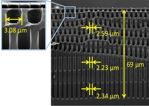
- Cell size 6 µm, pore diameter ~3 µm, pore depth 69 µm
- Surface cross-section area increases about 22
- Capacitance density of the stack (12 nm) is about 9.5 nF/mm2
- Capacitance density can be increased to 209 nF/mm2 in case of honeycomb-like 3D structure

Conclusions
• The ALD process has to be optimized to improve dielectric properties
• Electrical properties are good
• Aspect ratio has to be increased
REFERENCES
- P. Banerjee, I. Perez, L. Henn-Lecordier, S. B. Lee, and G. W. Rubloff, “Nanotubular metal–insulator–metal capacitor arrays for energy storage,” Nature Nanotechnology, vol. 4, no. 5, pp. 292–296, 2009.
- M. Gutsche, “Memory cell with a stacked capacitor,” Patent, Mar. 27, 2001, US 6,207,524.
- K. Kukli, M. Ritala, and M. Leskela, “Development of dielectric properties of niobium oxide, tantalum oxide, and aluminum oxide based nanolayered materials,” Journal of the Electrochemical Society, vol. 148, no. 2, pp. F35–F41, 2001.
- Y. Ma and Y. Ono, “Method of forming a multilayer dielectric stack,” Sep. 30 2003, US Patent 6,627,503.
- D.-S. Kil, J.-s. Roh, and H.-C. Sohn, “Hafnium oxide and aluminium oxide alloyed dielectric layer and method for fabricating the same,” May 26 2005, U.S. Patent App. 10/819,202.
- J. Azadmanjiri, C. C. Berndt, J. Wang, A. Kapoor, V. K. Srivastava, and . Wen, “A review on hybrid nanolaminate materials synthesized by deposition techniques for energy storage applications,” J. Mater. Chem. A, vol. 2, pp. 3695–3708, 2014.
- R. Y. Khosa, E. Thorsteinsson, M. Winters, N. Rorsman, R. Karhu, J. Hassan, and E. Sveinbj¨ornsson, “Electrical characterization of amorphous Al2O3 dielectric layers on n-type 4H-SiC,” AIP Advances, vol. 8, no. 2, p. 025304, 2018.
- J. Conley Jr, Y. Ono, R. Solanki, G. Stecker, and W. Zhuang, “Electrical properties of HfO2 deposited via atomic layer deposition using Hf(NO3)4 and H2O,” Applied physics letters, vol. 82, no. 20, pp. 3508–3510, 2003.
- I. Park, K. Ryu, J. Jeong, and J. Ahn, “Dielectric stacking effect of Al2O3 and HfO2 in metalinsulatormetal capacitor,” IEEE Electron Device Letters, vol. 34, no. 1, pp. 120–122, 2013.

