

This article written by Xiaoyan Yuan, KYOCERA-AVX Corporation discusses the case for electromagnetic simulation in mobile antenna design.
As the frequency, bandwidth, and the total number of radios within mobile devices increases, electromagnetic simulation in the earliest stages of the product life cycle has become a necessity. The modern mobile phone contains upwards of 13 antennas, including WiFi, cellular, Bluetooth, GPS, multiple mmWave modules, and NFC, to name a few. These antennas and radios compete for valuable real estate with other systems that are similarly pushed to their limits.
Battery capacity, processing power, non-volatile storage, and screen area comprise the leading cast of antagonists. To further complicate the story, the widespread adoption of 5G cellular has pushed radio frequencies into the sub-6GHz arena. Beyond that, in the 6-8 GHz band, ultra-wideband (UWB) devices are gaining traction for low power, short distance, real-time location systems. These advancements are making even the smallest of physical design choices exceedingly critical to achieve the expected performance.
Antenna Varieties
The physical design of RF antennas has drastically increased in complexity, encompassing multidimensional structures assembled from various materials. In passive antennas, one of the more common varieties is a piece of stamped and formed metal. A dual-band WiFi/Bluetooth example is shown in Figure 1.
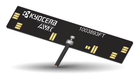
In some instances, the antenna must be physically distanced from other electronics or brought closer to the surface of an enclosure. Flexible printed circuit (FPC) antennas, similar to the one shown in Figure 2, can be an excellent solution due to their tunability and long feed wires.

The manufacturer simulates the meandering metal features to achieve the advertised gain, center frequency, bandwidth, radiation pattern, impedance, and other critical parameters. This type of antenna is soldered to a PCB and interfaced to a radio front end through a matching and tuning network.
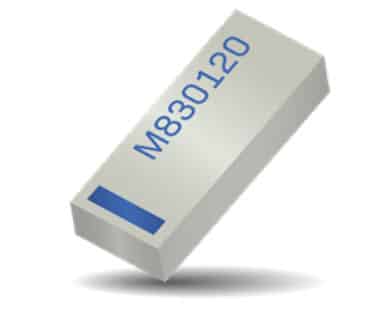
When PCB real estate is at a premium, designers often turn to antennas built from surface mountable ceramics. An example GPS antenna is shown in Figure 3, where a proprietary Isolated Magnetic Dipole™ (IMD) technology is used to limit interaction with its surroundings — a problem often faced by simpler monopole designs.
Such antennas can support GNSS bands L1/G1/B1/E1, for GPS, Galileo, GLONASS, and BeiDou, in a package of only 8.00 x 3.00 x 1.33 mm. Lastly, a fourth class of antenna for rigid off-board applications is worth mentioning. An example is shown in Figure 4 for a 6.0 – 8.5 GHz ultra-wideband radio where the antenna itself is patterned on rigid FR4 and connected via coaxial SMA.

Simulation for Suppliers
Given the complexity and variety of state-ofthe-art antennas, it is clear that they cannot be designed through manual calculations combined with iterative trial and error. Complex numerical simulation is required that incorporates the antenna shape and size and its various material properties, and all of their associated boundary conditions.
Simulation outputs can be compared to laboratory testing to validate assumptions and optimize the final design. This is only a small part of the story, however. Suppliers are also expected to support their customers’ design efforts with datasheets, application notes, and best practice guides.
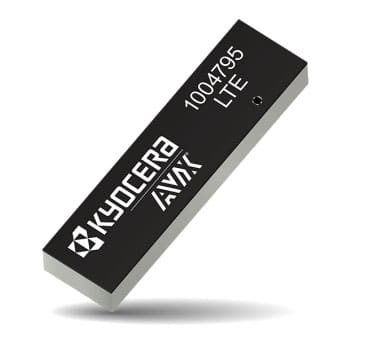
In many cases, the antenna itself is simulated with features allowing the end-user to fine-tune the performance in their particular application. An example of such an antenna with supplier provided designs for post-installation tuning is shown in Figure 5.
Along with this tuning feature, the supplier will provide a guide on how to bridge different combinations of pads to achieve shifts in frequency and radiation pattern. This may include simulations of return loss and antenna radiation patterns after various tuning modifications.
An example is shown in Figure 6 for an FR4 embedded LTE / 5G / LPWA antenna.
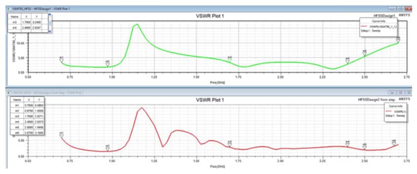
These types of before/after simulations greatly enhance the end user’s ability to properly tune a performant design, which should be the ultimate goal that every supplier strives for.
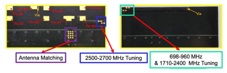
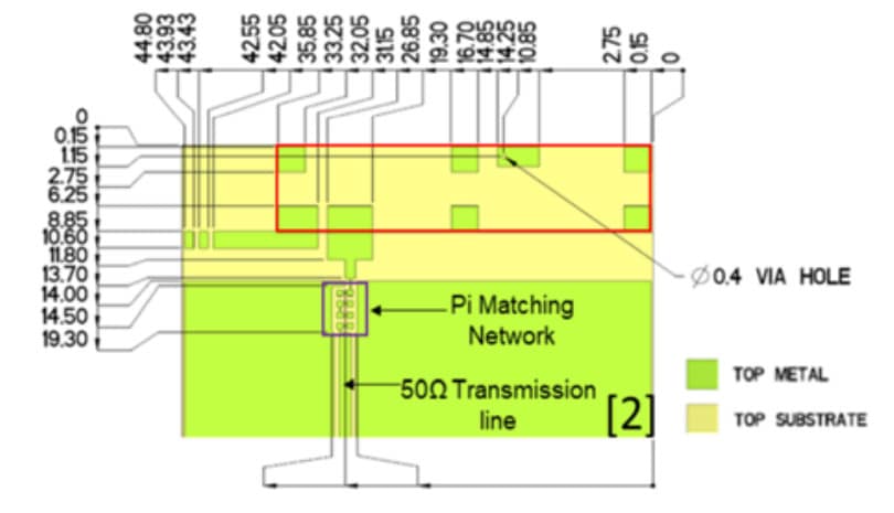
Similarly, many suppliers will simulate and include recommendations for PCB layouts specific to their antennas. This is especially common with stamped metal and ceramic components. An example is shown in Figure 7, where the landing pads, keep outs, stack up, and matching network are dimensioned for optimal performance of an embedded LTE antenna.
Simulation for Designers
While product designers can lean heavily on a supplier’s forethought in their antenna implementation, they will nevertheless endure numerous cycles of physical adjustment and electronic tuning to achieve the desired performance. This is especially true in many RF applications that have emerged with advancements in miniaturization. More and more radios are being embedded and collocated in places never before considered. Wearables, medical implants, and IoT sensors are just a few examples. Numerical simulation of antenna performance at the earliest stages of the design cycle is indispensable to realizing a high-quality, manufacturable product. their antennas. This is especially common with stamped metal and ceramic components. An example is shown in Figure 7, where the landing pads, keep outs, stack up, and matching network are dimensioned for optimal performance of an embedded LTE antenna.
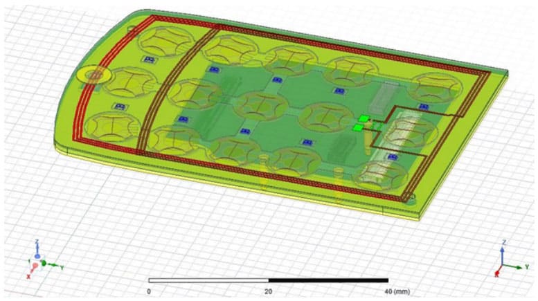
One real-world example is shown in Figure 8, where an NFC antenna was integrated into a mobile phone. The antenna traces meander around various other components, including other radios. Without simulation to inform the rest of the design, this antenna would likely perform poorly and require additional design cycles, potentially affecting the rest of the product.
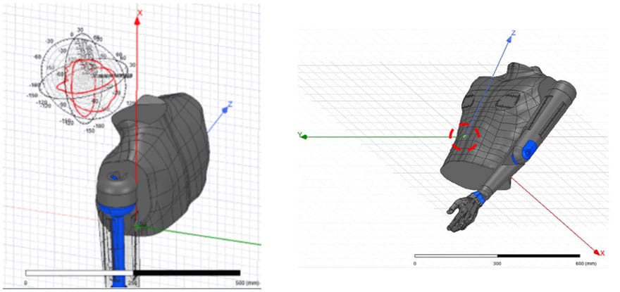
Another real-world example is shown in Figure 9, in which a wearable biomedical device is simulated at different locations and positions relative to the human body. The human computational models replicate the local tissue response of real people, perform a reliable estimation of antenna parameters, and allow designers to evaluate a variety of “what if” scenarios. Again, such a design would be nearly impossible without these advanced simulation tools and the models to support them. Interactions of materials, positioning, and interference would cripple antenna performance in all but a few idealized scenarios.
Conclusion
Today’s electronics market is driven to design products with multiple radios in a single box to deliver a rich user experience through complementary connectivity.
Bluetooth, Cellular, Wi-Fi, GPS, and many other protocols must be accommodated simultaneously. Simulation is an effective strategy to help the design engineer understand the broader picture of antenna utilization and predict radio issues in the early stage of product development.
KYOCERA AVX offers a wide variety of antenna products and design services to aid any RF venture.

