
source: Microwaves & RF news
Mar 14, 2017 Jack Browne | Microwaves and RF
Gallium-nitride (GaN) transistors are well known for their roles in RF/microwave amplification, but the active devices are also essential building blocks for high-speed power conversion and power supplies.
Recent testing of GaN-on-silicon (GaN-on-Si) enhancement-mode devices by Imec, in collaboration with Thales Alenia Space Belgium, has revealed that these devices are well suited for space applications, where high doses of radiation can degrade device performance. Testing showed consistent performance before and after irradiation with heavy ions and neutrons, as typically found in space applications such as satellites.
The measurements offer strong evidence of the suitability of the GaN-on-Si devices for space-based power conversion applications. Testing was conducted on Imec’s 200-mm GaN-on-Si process devices, which showed good radiation hardness and no permanent degradation in transistor characteristics following irradiation. Because the GaN devices are fabricated on silicon substrates, they are compatible with CMOS devices fabricated on silicon for simplified integration of power-conversion and computing circuitry. Measurements followed the framework of the European Space Agency (ESA) project ESA AO/1-7688/13/NL/RA, “GaN devices for space-based DC-DC power conversion applications.”
“These results are important to start using this promising technology for space applications,” noted Rudi Cartuyvels, executive vice president at Imec. “Also, it demonstrates that our 200-mm GaN-on-Si platform has reached a high level of technology readiness and can be adopted by industry.
“Thanks to innovations in transistor architecture and substrate technology, we’ve succeeded in making GaN devices on larger wafer diameters than used today, which brings lower cost perspectives for the second generation of GaN-on-Si power devices,” he added. “Imec is also looking beyond today’s technology, exploring novel substrates, higher level of integrations, and novel devices.”
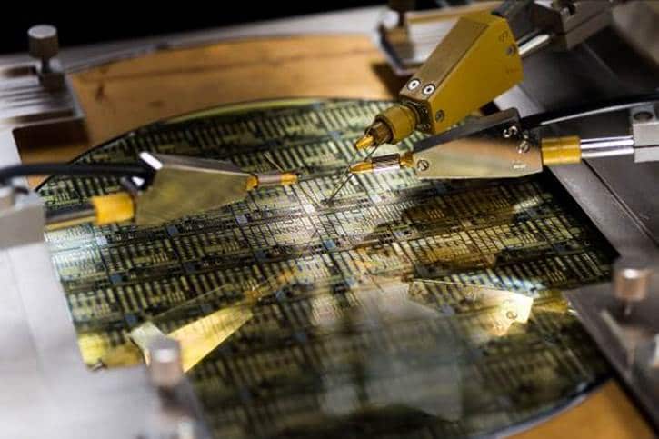
featured image: Automated wafer probes are measuring the electrical performance of DC power devices on GaN substrates. (Courtesy of Imec)

