
Source: EE Times article and EBN article
by Daniel West, Field Application Engineer, AVX and Ron Demcko, AVX Fellow
To-date, the evolution of electronic components such as capacitors, resistors, diodes, and RF filters has trended toward continued miniaturization while retaining as many parametrics as possible and, at times, adding functionality. Improvements across multiple scientific fields have contributed to these designs, but the most notable progress includes purer ceramic, tantalum, and thin-film materials and improved processes, such as closed-loop manufacturing (CLM).
These shifts have enabled extremely accurate computer-aided design (CAD) models which can be translated into marketable, real-world parts. Inventive combinations of other techniques, including packaging designs, fine copper terminations, and photolithography have further expanded components for miniature circuit designs.
Key drivers
OEMs and their electronics designers are looking for miniaturized parts to optimize circuit and system performance, satisfy physical design requirements, and improve product aesthetics. Smaller parts also typically operate at higher speeds with lower parasitics, making them more compatible with integrated circuit (IC) advancements.


Over time & markets
Miniaturized capacitor use has evolved from very specialized applications to more mainstream markets. Some highlights include:

- Defense: The Torpedo Data Computer (TDC) was one of the first electromechanical analog computers small enough to fit within a submarine and was used during WWII (1939–1945) to automatically track targets.
- Aerospace: Launch costs of roughly $10,000 per pound, extreme operating conditions, and the potential risk to human lives required capacitors to deliver improved functionality and utmost reliability in the most size- and weight-efficient packages possible.


- Consumer: Commercial versions of advanced defense, space-grade, and other high-reliability capacitors shrank living room radios down to portable boom boxes and then cassette, CD, and MP3 players; vacuum-tube televisions down into flat screens and phones; and rotary phones into wireless, mobile, and now smartphones, which contain around 1,000 MLCCs in slim, sleek, lightweight form factors with extensive functionality.
Enabling factors
- Reduced packaging/case sizes
- More accurate processing technologies

- Fine copper terminations (FCTs)
- Photolithography


- Closed-loop manufacturing processes
- Capacitor Consolidation: Achieving miniaturization by increasing capacitor functionality within their currently defined space.
- Enhanced material purity
- Design optimization via software modeling
Shrinking Large Components: Packaging Advancements
Component packaging advancements have emerged as key enabling factors of component miniaturization, as sizes have gradually decreased over time.

Some packaging technologies have been standardized by size, like the case sizes for rectangular passive components. With dimensional information built into the nomenclature, engineers can quickly and easily grasp the size difference between a 5025 and a 0201 capacitor without even seeing them. Combining improved packaging methods with capacitor material advancements, including thinner ceramic layers or finer grain tantalum power, has enabled diminished case sizes with capacitance values comparable to larger case sizes.


Shrinking Large Components: RGCs
Reverse geometry capacitors (RGCs) are an excellent example of size reduction. RGCs modify MLCC terminations to shorten the distance between terminals and reduce the length of the inductive loop created at high frequencies to achieve lower ESL. Although the physical case size isn’t reduced, the altered case facilitates smaller low ESR solutions.


Shrinking Large Components: Stacked Capacitors
TurboCap MLCCs were developed using advancements made in processing BME MLCCs and are packaged in slightly modified versions of the lead frames used for horizontally stacking MLCCs. TurboCap MLCCs achieve high capacitance in a small area (high CV) by vertically stacking capacitors, which reduces the footprint and improves ESR and ESL. 

They also utilize a dual in-line package (DIP) in through-hole or surface mount configurations to provide stress relief for the ceramic elements. The leads effectively isolate the stacked caps from the board to minimize thermal and mechanical stresses encountered during assembly, temperature cycling, and other environmental conditions.
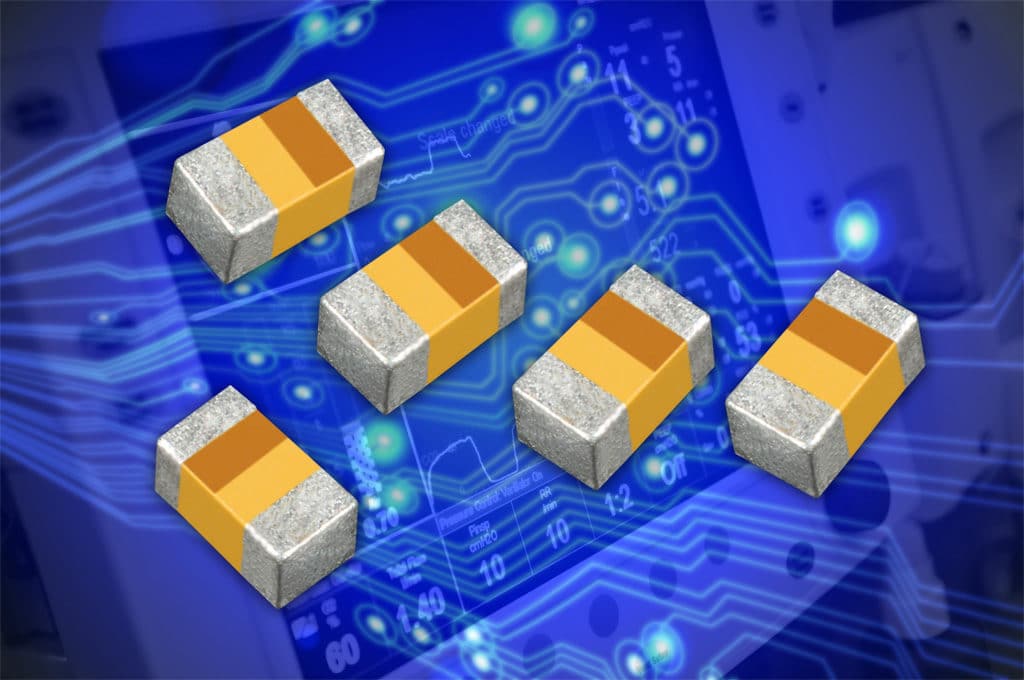
AVX’s TurboCap Series. The black variants are potted.
Thanks to their unique packaging, TurboCaps provide smaller, lighter, lower ESR, and higher-reliability solutions than the large, radial-leaded aluminum electrolytic (AL-EL) capacitors often used as I/O stage filters in switched mode power supplies (SMPS). A typical 27μF TurboCap exhibits 2mΩ ESR at 100KHz.


They also exhibit low parasitic losses and improved stability across temperature and frequency compared to AL-EL capacitors, allowing designers to replace larger AL-EL capacitors with much lower value TurboCaps. A 1:10 ratio isn’t unheard of, meaning that a 1μF TurboCap can replace up to 10μf AL-EL.


Shrinking Large Components: Packaging Changes
Component footprints can also be reduced by simply switching package sizes. For example, a common package for diodes, the SOT23, replaced with a small-case-size package typically used for rectangular passive components could offer incredible space savings.
This option isn’t always viable, but it’s not altogether uncommon. AVX’s GiGuard bidirectional transient voltage suppression (TVS) diodes utilize miniature, leadless EIA 0201/0402 component packaging technology to provide advanced ESD protection for sensitive ICs in space-constrained, high-speed communication applications. They have low clamping voltages (<12V) and capacitance values (0.3pF) and meet IEC 61000-4-2 Level 4 (±15KV air/contact) and IEC 61000-4-4 electrical fast transient (EFT) (20A, 5/50ns) standards.


Fine copper termination technology
As case sizes for standard SMD ceramic capacitors decrease, their terminations begin to dominate their PCB surface area. Fine copper termination (FCT) technology reduces, if not eliminates, the footprint reserved for soldering leads by attaching planar copper lead-frame substrates to the bottom of components. FCTs enable high-density terminations, reduce PCB solder variability, and free up valuable PCB surface area, which is especially useful in high-density applications.
Achieving ultraminiature capacitors
Material advancements, alternative terminations, and improved processing technologies have led to the development of even smaller, ultraminiature capacitors. Ultraminiature MLCCs were achieved through material advancements including smaller particle size, thinner dielectrics, and alternative termination technologies.
Higher-voltage tantalum capacitors (e.g., 35–63V) require larger particle sizes and thicker dielectrics to achieve high capacitance values. Lower-voltage tantalum (<16V) can achieve high capacitance with thinner dielectric materials and finer tantalum powder particles powders. This is due to improvements in pressing and sintering high CV powder and firing and finishing small anodes. Tantalum capacitors also utilize alternative terminations to achieve space savings.
Undertab terminations
Tantalum Polymer (TaPoly) capacitors utilize undertab terminations for footprint reductions. Undertab terminations are routed to the cathode and anode, within the housing of a tantalum capacitor, to capitalize on the existing volume of the capacitor housing and reduce the amount of PCB surface area required.
TaPoly caps are extremely stable. They have inherently low ESR; no voltage coefficient; wide frequency resilience due to an absence of acoustics at low frequencies; and capacitance retention at high frequencies. The also retain high volumetric efficiency (CV/cc). TaPoly caps have benign failure modes due to optimized polymer deposits on the Ta anodes. Ideal applications span a wide range of switching, filtering, decoupling, timing, and back-up circuits that require parametrically stable capacitors.


Achieving Ultra-miniature Capacitors: Photo-lithography Technology
Advancements in photolithography technology have dramatically improved the viability of miniature, ultra-low-profile, thin-film capacitors and filters. These are primarily used in wireless applications sensitive to component variability at high frequencies, such as automotive collision detection modules.
Photolithography achieves miniature capacitors and filters with accurate part-to-part and lot-to-lot parametric repeatability and tight tolerances, which increases production yields and performance reliability. Equipment is installed in Class 100 or Class 1,000 clean rooms and has 2.0µm line definition accuracy, which enables the construction of identical dielectric depositions in thin film substrates.
This process also uses purer-than-standard electrode material and only a single layer of dielectric. Since dielectrics employed in multilayer constructions must be accurately spaces, the single-layer construction reduces component variability. It also avoids the firing processes common to ceramic capacitor construction, which prevents heat distribution variances.


Unique solutions combine packaging advancements & FCTs with closed-loop manufacturing materials


A unique solution for achieving miniature capacitors with very high operating temperatures (230°C), stable performance, and long operating lifetimes (e.g., for use in expensive drilling heads and sensors) is to combine ceramic packaging and tantalum material. Tantalum capacitors with a manganese oxide cathode are mechanically robust and temperature resilient to 230°C with the addition of ceramic packaging.
Ceramic is also mechanically robust and happens to make a great hermetic seal. As such, it can be filled with nitrogen gas and used to encapsulate tantalum caps to mitigate the degenerative effects of oxygen and humidity on the tantalum. To ensure that this combination delivers long operating lifetimes, a patented closed-loop manufacturing (CLM) process is used to remove raw material exhibiting trends toward excessive thermal parametric shifts.
When combined with advanced packaging, undertab terminations, and the snuggest possible ceramic hermetic seal (e.g., AVX’s THH Series), CLM materials can boost capacitor operating temperatures to 230°C.

AVX SuperCaps also use patented CLM processes to match material parametrics and achieve either low ESR or low leakage current modules, in addition to optimized sealing methods for extended lifetimes.
Capacitor consolidation: Miniaturization via improved functionality
Capacitor size reductions can also be achieved by increasing the functionality of a same-sized capacitor with fewer capabilities. Physical miniaturization can pose significant component design challenges,and pushing the limits of electronic component functionality can be even more difficult.
This process requires a thorough understanding of the limitations of the raw materials used in capacitor manufacturing, including copper, nickel, silver, gold, tantalum, barium titanate, and alumina. The improved ability to remove impurities from raw materials and process them using closed-loop manufacturing (CLM) techniques plays a key role in component capabilities, reliability, and electrical and thermal stability.


For example, the density of barium titanate (BaTiO3), which is used in ceramic capacitors, has a positive correlation to its permittivity (εr), increasing capacitance C = [(εrε° x A)/d] at the cost of reducing the temperature band where this value is constant. Using very fine grain tantalum powder increases the surface area (“A” in the capacitance equation) during electrolysis and achieves a very high CV/g, which offers size and weight advantages, but reduces the amount space available to grow a thick dielectric layer and thus reduces the breakdown voltage.

Capacitor consolidation: Miniaturization via Improved functionality/ CAD


Combining the latest CAD software advancements with improved packaging, termination, photolithography, and termination techniques, as well as consolidation capabilities, can result in incredibly innovative solutions.

Supporting Technologies
The purer materials that facilitate accurate CAD modeling for components also enhance circuit reliability in size-constrained circuits where RF component power handling is important.
Thin-film chip resistors offer efficient, low-power RF solutions by tightly controlling the pattern of resistive material deposited onto a substrate, which minimize parasitic impedances, while an understanding of the resistive and substrate material heat conduction properties, made possible via advanced material processing procedures, enable the higher power handling.


Power resistor

One of the smaller high-power resistive products AVX offers is the RP9 Series, which has a surface-mount footprint of 2.54 x 5.08mm. Impedance values range from 10–200Ω (50Ω nominal) at a tolerance of ±2% and up to 40W power handling with an operating temperature range of -55°C to 150°C and resistance values up to 4GHz. These parts were achieved by combining a thorough understanding of heat conduction across substrates with advance resistor material processing.
Wire bond resistors
AVX’s WBR Series wire-bond resistors employ the same material advances in an even smaller, ultraminiature 0202 chip outline ideal for hybrid circuits in medical implantable, high-reliability microelectronics, multi-chip module, and RF/microwave applications. They offer customizable resistance values, are laser trimmed for tolerances down to 0.5% of specified value, and were developed using a combination of proprietary thin-film processing advances, including miniature depositions of resistive material in conjunction with advanced terminations, in addition to clean room advancements, process control and design improvements, and enhanced material purity.


Q-Bridge thermal conductors
Smaller components in increased densities can present a thermal problem when there is no efficient method of redirecting heat away from vital components. Q-Bridge Series thermal conductors from American Technical Ceramics (ATC) provide cost-effective solutions in standard EIA case sizes down to 0402. Q-Bridge conductors improve circuit reliability by efficiently directing heat to thermal ground planes, heat sinks, or any other thermal point of interest, and their low capacitance — achieved via the impedance minimizing construction of the pure, precisely processed materials used — makes them virtually invisible at RF/microwave frequencies.
For example, thermal conductors provide a safer alternative to increased trace widths for redirecting heat in a high-voltage power transistor, as the latter introduces arcing risk. This technology is a result of RF power resistor development. Heat conduction across substrates coupled to terminations made these miniature SMT heat sinks possible.


