
source: EDN article, Tony Armstrong -March 19, 2016
Switching regulators are a popular choice for many power conversion supplies due to their size, output flexibility and efficiency advantages. Conversion efficacy of these supplies can now attain 98% levels, depending on operating conditions. Nevertheless, despite these advantages, they necessitate compromising on other parameters, one of the most difficult of which is noise.
Background
What is switching regulator “noise?” To have a better understanding of this term, let’s start with the fact that switched mode power supplies create wideband harmonic energy. This undesirable energy manifests itself in two components, radiated and conducted, which are routinely labelled in the industry as “noise.” However, this is really a misnomer, since a switching regulator’s output “noise” is not noise at all, but coherent high frequency residue directly related to the regulator’s switching. The correct term for this phenomenon is electromagnetic radiation, or more commonly, EMI. And yes, it comes in both radiated and conducted forms.
Since quiet, well-regulated power supplies are important for optimum performance in many circuit applications, it is important to be able to mitigate any noise generated as part of this conversion process. An obvious way to attain this is to simply use a linear regulator. However, although they supply quiet power supply rails, their conversion efficiencies are poor at high step-down ratios and this can lead to thermal issues with the design in high output current applications.
Correspondingly, switching regulators usually have higher conversion efficiencies than linear regulators, leading to simpler thermal design when high output currents are required by the end application. It is well understood that component selection and circuit board layout can play a significant role in determining the success or failure of virtually all power supplies. These aspects set their functional EMI and thermal behavior. For the un-initiated, switching power supply layout may seem like a “black” art, but it is in fact a basic aspect of a design often overlooked in the early stages of the process.
Since functional EMI requirements always have to be met, what is good for functional stability of the power supply is also usually good for its EMI emissions, too. Furthermore, good layout from the beginning does not add any cost to the design and can actually provide cost savings by eliminating the need for EMI filters, mechanical shielding, EMI test time and numerous board revisions.
Moreover, the potential problems of interference due to noise can be exacerbated when multiple DC/DC switchmode regulators are used in a design to generate multiple rails of if they are paralleled for current sharing and higher output power. If all are operating (switching) at a similar frequency, the combined energy generated by multiple regulators in a circuit is then concentrated at one frequency. Presence of this energy can become a concern, especially if the rest of the ICs on the printed circuit boards (PCBs), as well as other system boards are close to each other and susceptible to this radiated energy.
This can be particularly troubling in industrial and automotive systems that are densely populated and are often in close proximity to electric noise generating sources, such as mechanically switched inductive loads, PWM drive power outputs, microprocessor clocks and contact switching. Furthermore, if switching at different frequencies, intermodulation products can alias into sensitive frequency bands.
Switching Regulator Emissions
In industrial, medical and automotive environments, switching regulators usually replace linear regulators in areas where low heat dissipation and efficiency are valued. Moreover, the switching regulator is typically the first active component on the input power bus line, and therefore has a significant impact on the EMI performance of the entire product design.
Conducted emissions ride on the wires and traces that connect up to a product. Since the noise is localized to a specific terminal or connector in the design, compliance with conducted emission requirements can often be assured relatively early in the development process with a good layout or filter design as already stated.
Radiated emissions are a different matter altogether. Everything on the board that carries current radiates an electromagnetic field. Every trace on the board is an antenna and every copper plane is a resonator. Anything, other than a pure sine wave or DC voltage, generates noise all over the signal spectrum. Even with careful design, a power supply designer never really knows how bad the radiated emissions are going to be until the system is tested. And radiated emissions testing cannot be formally performed until the design is essentially complete.
Filters are often used to reduce EMI by attenuating the strength at a certain frequency or over a range of frequencies. A portion of this energy that travels through space (radiated) is attenuated by adding metallic and magnetic shields. The part that rides on PCB traces (conducted) is tamed by adding ferrite beads and other filters. EMI cannot be eliminated but can be attenuated to a level that is acceptable by other communication, signal processing and digital components. Moreover, several regulatory bodies enforce standards to ensure compliance in both industrial and automotive systems.
Modern input filter components in surface mount technology have better performance than through-hole parts. However, this improvement is outpaced by the increased demands created by today’s high frequency switching regulators. The low minimum on and off times required at higher operating frequencies result in higher harmonic content due to the faster switch transitions, thereby increasing radiated noise. However, these high switch edge rates are needed to get higher conversion efficiencies. A switched capacitor charge pump does not exhibit this behavior since it operates at much lower switching frequencies and most importantly can tolerate slower switching transitions without degradation in efficiency.
Savvy PCB designers will make the hot loops small and use shielding ground layers as close to the active layer as possible. Nevertheless, device pin-outs, package construction, thermal design requirements and package sizes needed for adequate energy storage in decoupling components dictate a minimum hot loop size. To further complicate matters, in typical planar printed circuit boards, the magnetic or transformer style coupling between traces above 30MHz will diminish all filter efforts since the higher the harmonic frequencies are, the more effective unwanted magnetic coupling becomes.
An Alternative Solution to EMI Issues
The tried and true solution to EMI issues is to use a shielding box for the complete circuit, and even then, a shield does not prevent coupling to sensitive circuits inside the box. Of course, this adds cost, increases required board space, makes thermal management and testing more difficult and introduces additional assembly expense. Another frequently used method is to slow down the switching edges. This has the undesired effect of reducing the efficiency, increasing minimum on, off times, and their associated dead times and compromises the potential current control loop speed.
A few years ago, Linear Technology introduced our LT8614 Silent Switcher® regulator, which delivers the desired effects of a shielded box without using one, while also eliminating many of the above mentioned drawbacks. Nevertheless, in some noise applications, power supply designers simply do not like to use inductor-based regulators due to their associated EMI emissions. At the same time, the use of a linear regulator (aka LDO) may be precluded due to its relatively low conversion efficiency and need for heat sinking. As a result, they turn to a common alternative known as a charge pump.
Charge pumps have been around for decades, and they provide DC/DC voltage conversion, using a switch network to charge and discharge two or more capacitors. The basic charge pump switch network toggles between charge and discharge states of the capacitors. As shown in Figure 1, C1 the “flying capacitor” shuttles charge, and C2 the “reservoir capacitor” holds charge and filters the output voltage. Additional “flying capacitors” and switch arrays enable multiple gains.


Figure 1: Simplified Charge Pump Block Diagram of a Voltage Inverter
When switches S1 and S3 are on, or closed, and switches S2 and S4 are off, or open, the input power supply charges C1. During the next cycle, S1 and S3 are off, S2 and S4 are on, and charge transfers to C2, generating VOUT = – (V+).
However, until recently, charge pumps have had limited input and output voltage ranges, which has limited their use in industrial and automotive applications where inputs up to 40V or 60V are commonplace. However, this is now changed with the introduction of high voltage charge pumps from Linear Technology.
High Voltage Charge Pumps
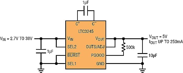
The LTC3245 is a buck-boost regulator that dispenses with the traditional inductor and uses a switched-capacitor charge pump instead. Its input voltage range is 2.7V to 38V, and it can be used without a feedback divider to produce one of two fixed output voltages, 3.3V or 5V, or programmed via a feedback divider to any output voltage from 2.5V to 5.5V. Maximum output current is 250mA. The LTC3245 is capable of regulating a voltage above or below the input voltage, allowing it to satisfy automotive cold crank requirements, for example. See Figure 2 for its complete schematic.

Figure 2: LTC3245 Schematic Delivering a Fixed 5V Output from a 2.7V to 38V Input
This charge pump is capable of achieving efficiencies of 80% when delivering 5V at 100mA from a 12V source, almost two times higher than that of a linear regulator, making it possible to avoid the space and cost requirements of an LDO with a heat sink. It generates almost three times lower power loss at full load versus an LDO. See Figure 3 for the LTC3245 efficiency and power loss curves.

The LTC3245 also has excellent radiated and conducted EMI performance, as show in Figures 4a and 4b. These measurements were taken in a micro chamber in accordance with CISPR22 and CISPR25. As can be seen, when properly decoupled, the LTC3245 does not present any issue when striving to meet government regulations for radiated and conducted emissions.

Figure 4: Radiated (a) and Conducted (b) Emissions of the LTC3245
In many industrial, medical and automotive applications, a dual-polarity supply is often needed to operate electronics such as op amps, drivers and sensors. However, there is rarely a dual-polarity supply available at the point of load. It was because of this need, and the lack of a simple-to-use solution, that Linear Technology developed the LTC3260.
The LTC3260 is an inverting charge pump DC/DC converter with dual low noise LDO regulator followers that can produce positive and negative supplies from a single 4.5V to 32V input power source, as illustrated in the Figure 5 complete schematic. It can switch between high efficiency Burst Mode® operation and low noise constant current frequency mode, allowing the designer to make an optimum trade-off for the application.
The LTC3260 can supply up to 100mA from the inverted input voltage at its charge pump output, VOUT. This VOUT also serves as the input supply to a negative LDO regulator, LDO-. The charge pump frequency can be adjusted between 50kHz and 500kHz with a single resistor. Each of the LTC3260’s LDOs is capable of supporting up to 50mA loads. And, each LDO has a dropout voltage of 300mV at 50mA, and an output resistor divider network allows the setting of the output voltage. When both regulators are disabled, the shutdown quiescent current is only 2µA.

Figure 5: A 12V Input Supply to ±5V Outputs
Conclusion
It is well known that EMI considerations for industrial, medical and automotive environments require careful attention during the initial design process in order to ensure that they will pass EMI testing once the system is completed. Until now, there has been no sure fire way to guarantee that this could easily be attained with the right power IC selection for all but very low power systems.
Recent introductions of low EMI regulators and DC/DC converters from Linear Technology include an extensive line of linear regulators, as well as the LT86xx Silent Switcher buck converters. Now our growing family of high voltage charge pumps offer a third choice. These products provide much higher efficiency and lower power loss when compared to linear regulators and do not require the compensation, layout, magnetics and EMI issues associated with switching regulators.

