
source: TTI Market Eye article
06/02/2017 // Dennis M. Zogbi shares his view of the MLCC shortages at his article for TTI Market Eye.
Introduction
High capacitance base metal electrode multilayered ceramic chip capacitors (MLCC) have been the focal point of electrostatic capacitor technology for more than 25 years. The stacking of advanced dielectric materials and nickel electrode powders in the finished MLCC creates a component with extremely high capacitance that extends the product offering well into the higher priced electrolytic range. The materials stability of ceramics and lower cost structure of the MLCC is attractive to design engineers, as is the robust performance of ceramics in a circuit. Also, the displacement of palladium in PGM type MLCC is also an attractive way to distance a vendor from a volatile and precarious supply chain while lowering overall costs. The mass production of high capacitance MLCC using BME systems began in 1993 (although the original MLCC prototypes using base metal electrodes were first produced as far back as 1972) and continues to this day and remains one of the most successful growth stories in the entire passive components industry to date.
2017 HIGH Cap BME MLCC Shortages
In 2017, a shortage of MLCC, especially high capacitance MLCC BME MLCC began, prompting Paumanok to update this study. The reasons that high cap BME MLCC are reluctant to add capacity is because of a slowdown in the unit consumption in handsets, due to saturation of handsets into global populations. Only slow unit growth is expected as more features in future handsets increase MLCC content per phone; however, the added growth realized by continued penetration into global populations is largely over, limiting overall unit demand in handsets going forward.
The increasing lead times for ceramic chip capacitors is best illustrated in Paumanok Publications, Inc., slide (shown below) that shows how lead times for ceramic chip capacitors of all case sizes are increasing after years of symmetrical month-to-month consumption.
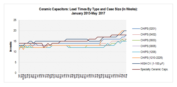

Source: Paumanok Publications, Inc. Monthly Market Report
The Two Primary Technical Economic Maxims Associated with MLCC
There are two primary technical factors that impact the economics of capacitors 1) capacitance is required for almost all electronic circuits and 2) capacitance is equivalent to the physical size or available surface area of the finished component, which makes raw materials used in the production of capacitors key to cost, price and technical advancement. For MLCC, the dielectric layer is stacked on top of the electrode and built up to more than 1000 layers. Therefore the focus of research and development as it applies to MLCC is to improve the capacitance value per cubic centimeter of MLCC by manipulation of the ceramic dielectric material and the nickel paste and to improve upon the process by which these materials are dispersed. This improves yield ratios and advances the technology forward.
Relationship between Capacitance and Available Surface Area in MLCC
The other technical-economic maxim that is important for the reader to understand is that capacitance is equivalent to the finished size of the finished component, or more to the point, capacitance is directly proportional to the available surface area contained in the finished capacitor (similar parameters apply to resistors and inductors as well).
In the above example of capacitance technology, the similarity is that the solution of capacitance is ultimately reliant upon the raw material, but most importantly, it is the ability for that raw material to be “manipulated” into a format that can be used by the customer. Since MLCC represent the largest market with respect to capacitors by type, the technology with the largest amount of research and development dollars (as a percentage of total revenues) is in stacking of ceramic dielectric materials. Subsequently, the technology innovation in ceramic chip capacitors has been absolutely revolutionary from 1993 to 2017. Moreover, it has been the true application of “nanotechnology” as it applies to both ceramic dielectric materials and to electrode powders and pastes that has enabled the advancement of available surface area in MLCC. In fact, it has been the ability for engineered materials producers and the captive in-house capabilities of MLCC manufacturers to process ultra-fine “nano-sized” titanium and barium powders (for the dielectric) and nickel (for the electrode) into increasingly small, spherical particle sizes that has been the building block for advancements in available surface area. The “consistency” of particle sizes, as well as the ability for the capacitor manufacturer to cast these materials into ceramic “tapes” and to apply consistent layers of electrode pastes; and to effectively “stack” these interposing layers (in some instances- more than 1000 layers), which has enabled the MLCC industry to grow at a rate that exceeds other capacitor types. The reader should understand that the importance of raw material innovation, as well as the application of raw materials in the global ceramic capacitor industry has been instrumental in its success as a dielectric, and will continue to be the basis for innovation in the MLCC industry for years to come.
The illustration below shows the basic design of the MLCC with the stacked appearance, whereby electrode material is deposited upon ceramic dielectric material to create a stack of layers, and the finished capacitor body is termination by dipping in precious or base metals.
Illustration 1: The Stacked Layer Construction of The Modern MLCC
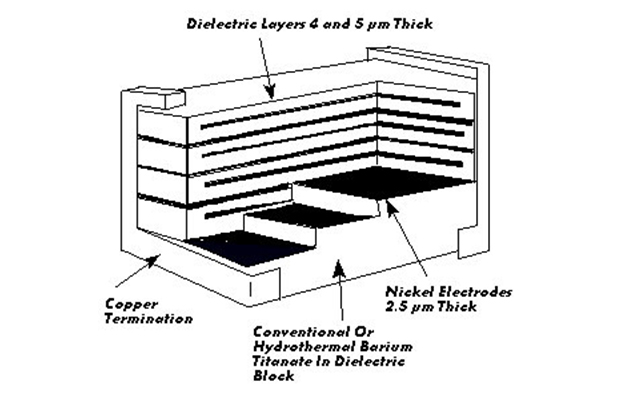
Source: Dennis M. Zogbi The key to the high capacitance MLCC market competition in 2017 is the ability for manufacturers to stack increasingly larger number of layers in the same footprint.
Ceramic Capacitor Metallization
Metallization for multilayered ceramic chip capacitors has undergone a radical change over the past ten years. Beginning in 1993 (at TDK Corporation) the displacement of palladium bearing electrodes with nickel electrodes began although work in nickel electrodes goes back to the 1970s at Philips). This limited the reliance on the expensive palladium metal, and displaced it with a more stable non-noble, or base metal (nickel). This change was revolutionary because it lowered production costs, while enabling MLCC manufacturers to cost effectively produce MLCC in much higher capacitance ranges and compete with tantalum and other electrolytic capacitors. In 2017 close to 85% to 90% of all MLCC produced will be base metal in nature. Subsequently, palladium consumption in the MLCC industry has declined to about 25% of its former usage in terms of volume over a 16 year period.
Both electrodes and termination pastes are created from powders that are mixed with solvents and binders to create a paste that can be spread out on top of a dielectric layer. The application of nano-technology principals on metals enabled the development of increasingly more sophisticated metal powders and pastes over time.
Ceramic Dielectric Materials
The other primary raw material is the ceramic dielectric powder which gets converted into carrier tape for the electrode metal paste. The ceramic dielectric materials are based upon the basic building block of barium titanate. Barium titanate in turn is made from barium carbonate and titanium dioxide. Many MLCC manufacturers have the ability to make their own barium titanate in-house, but will source the merchant market for specialty formulations. Special formulations are required to create capacitors with tight tolerances, or for high voltage or high frequency. There is a considerable merchant market for ceramic dielectric materials worldwide.
With the advent of mass MLCC production with base metal, significant developments have also been made in advanced dielectric material production methods. The key here is to produce ceramic dielectric powders with very small, spherical or tetragonal shapes that have consistent particle sizes throughout the mix. Advanced materials production methods such as alk-oxide, hydrothermal and even sol-gel techniques are employed to control ceramic dielectric material particle sizes.
Ceramic dielectric powders are mixed into pastes, usually with either an aqueous or alcohol based solvent and combined with a plasticizer and a binder material. This creates a slurry that can be extruded with Doctor Blade and dried into dielectric sheets for stacking.
Gaps and Showstoppers
Challenges with Stacking Thin Layers Creates New Lead Time Realities:
The gaps and showstoppers that have sprang up over time and hampered the technical growth in the advanced development of MLCC, has to do with the unique nature of attempting to create extremely thin and varying layers of ceramic and metal.
One consistent problem noted over time has been in the agglomeration of nickel electrode powders while converting the electrode powder into paste and spreading that paste evenly across the ceramic dielectric tape. The creation of increasingly small but incredibly uniform spherical shapes is an challenging technical process, with even the slightest variation on particle size creating irregular patterns that can lead to poor yields. These problems magnify as the particle sizes become smaller; and the component manufacturer is constantly trying to create increasingly smaller particles that can be stacked at increasingly thinner layers. This creates undesirable yield ratios in the production of next generation passive electronic components. In fact, a major semiconductor manufacturer has pointed out that MLCC manufacturers have largely been successful in expanding the available voltage ranges in high capacitance BME MLCC, but have had difficulties in successfully expanding the available capacitance value because of the extremely thin layers of both the metal electrode and the ceramic dielectric.
In the ceramic dielectric arena, the problems with the precipitation of ultra-small particles manufactured from titanate based (or similar) compositions, are similar to those experienced with nano-metal technology. This includes the agglomeration of particles in the final slurries and tapes, which create what one major Japanese manufacturer of MLCC described to me as “microscopic pinholes and tears that lead to part failures.”
A Way Forward
Manufacturers of MLCC have made remarkable inroads in the application of nano-materials into electronic components, and based upon my research believe that thick film solutions that have been applied to the production of MLCC over the past 25 years still continue to see breakthroughs that move the technology along over the next 25 years but at a much slower pace. Instead, the data suggests that manufacturers of MLCC will establish a foothold in a specific leading edge microfarad value, and then expand the technology laterally, by offering varying voltage ratings at different “performance with temperature” characteristics and at diminishing component “thicknesses.”
As the layers get thinner the advancement of the technology has slowed leading to a new reality in lead times for high capacitance MLCC. In a recent study I pointed out how advancements in X5R MLCC have been nothing less than astounding between 2005 and 2017, with one capacitor manufacturer, Taiyo Yuden, announcing the development of a 470 microfarad X5R MLCC. This incredible achievement sets a new benchmark in the cycle of capacitance development, but other manufacturers have not been able to achieve this new goal, and other vendors have seemingly stopped trying. This is creating a gap in technology because the portability and functionality of future electronic devices warrant a need for higher capacitance in a smaller case size.
One of the ways forward in the future will be greater control over raw materials by the MLCC manufacturers. The importance of the marriage of ceramic and metal in the stacked component are paramount to its continued development. To date however, no MLCC manufacturer has captive control over nickel electrode powder AND ceramic dielectric material. In fact, all key materials for the development of extremely high capacitance MLCC at the cutting edge still comes from the merchant market outside the electronics industry.
Also, nickel technology far exceeds that of ceramic technology when applied to electronics because of the massive amounts of research and development funding coming from the battery market. The CEO at the top vendor of nickel electrode powder in the world noted to me once that their ability to produce small spherical coated shapes consistently at a microscopic level far exceeded that of ceramic dielectric materials, and this would be a continued problem for years to come as the technology progressed. He also noted that the availability of extremely small particle sizes in nickel enabled the market to progress faster by baiting the interest of the manufacturers with “what could be.” But the reality was that ceramic technology lagged behind nickel technology and until that gap was filled, the market continued to struggle with advancing in a cohesive way. In hindsight, this is exactly what is happening today, and why lead times for MLCC will have to increase to a new level of reality going forward.

