
Switched-mode power supplies (SMPS) have the advantage of high efficiency compared to traditional low-dropout (LDO) regulators. Due to its switching nature, a SMPS emits noise at its switching frequency and its harmonics. This article illustrates the procedure of designing filtering to achieve ultra-low output voltage noise with SMPS regulators.
Single-stage capacitive filter is commonly used for DC/DC converter applications. Low ESR ceramic capacitors are utilized to meet output voltage ripple specifications. The single-stage capacitive filter is sufficient for applications that requires no less than 1-2mV of output voltage ripple. For applications such as RF ADC and DAC applications where it is necessary to meet less than 1mV ripple, a second-stage LC filter should be used to effectively suppress the switching noise.
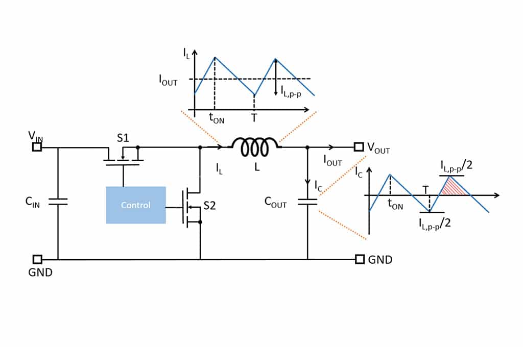
Single-Stage Filter Design
A synchronous buck converter consists of an input capacitor CIN, two switches (S1 and S2) with their body diodes, an energy storage power inductor (L), and output capacitors (COUT). The input source provides energy to the power inductor (L) and the load when S1 is turned on and S2 is turned off. During this period, the inductor current rises. The energy stored in the inductor is transferred to the output capacitor and load when S2 is on and S1 is off, causing the inductor current to drop. The switching behavior of the buck regulator causes the output voltage to fluctuate. The output capacitors (COUT) is placed at the output to smooth the output voltage under steady state. The output capacitor reduces the output voltage ripple by providing a low impedance path for the high-frequency voltage components to return to ground.


In the subsequent development, it is assumed the buck converter operates under continuous conduction mode (CCM) for output voltage ripple minimization. The inductance of L is designed to meet inductor current ripple requirement. The minimum inductance of L is determined as:


Where VIN and VOUT represent the input and output voltage, respectively, ![]()

The output capacitance is selected to ensure that the output ripple is below the specified peak-to-peak value. For a single-stage capacitive filter, an minimum output voltage ripple of 1mV to 2mV can be achieved.
Under steady state, the net electric charge delivered to the capacitor is zero within one switching period. The capacitor charge of the shaded area in Figure 1 is calculated as:


Where T is the period of one switching cycle. By definition, the capacitor charge in a given period is also can also be expressed as:
![]()

Equating Equation (2) and Equation (3), the minimum capacitance to achieve the required output peak-to-peak voltage ripple (VOUT,p–p) is determined as:


Ideally, the noise shunt capability can be increased by paralleling more output capacitors. Practically, the output capacitors are laterally placed on a PCB. Adding more output capacitors on a PCB would introduce additional parasitic inductance and AC resistance to the shunt path and thus reduce the effectiveness of bypassing the switching noise.
A typical PCB layout of an MPS power module, which integrates optimized inductors to simplify the power converter design, is shown in Figure 2. In the PCB layout of the MPM3833C, a wide copper plane is used for the output power path to minimize power losses. The output capacitors are placed along the output current path. As shown, as more capacitors are placed on the output plane, the distance from the additional capacitor to the output pin of the power module increases. Consequently, more parasitic inductance is involved in the output capacitor that is further away from the power module. Adding more output capacitance become less and less effective and eventually, the shunt loop is dominated by parasitic inductance.


Figure 2: Typical PCB Layout for MPM3833C Power Module
To demonstrate the impact of loop parasitic inductance, an MPM3833C with various output capacitors issimulated using Simplis. It is assumed that each additional output capacitor introduces an additional 0.5nH of parasitic inductance to the bypassing loop. Figure 3 illustrates the output ripple of the power module with one 22µF capacitor. The bypassing capacitor effectively reduces the output ripple to around 3mV at 5V input, 1.2V output, and 2A load.


Figure 3: Output Voltage Ripple of MPM3833C with One 22µF Output Capacitor
To further reduce the output voltage ripple, one additional 22µF output capacitor is place at the output. Since the new capacitor has to be placed further away from the power module, the parasitic inductance involved with the new capacitors is 1nH. The simulated output voltage ripple is shown in Figure 4a where the output voltage ripple is reduced to 2mV. Compared to the waveform shown in Figure 3, where one 22µF output capacitor effectively brings down the output voltage ripple to 3mV, the additional one 22µF capacitor is less effective. Figure 4b shows the output voltage ripple with one more 22µF capacitor (total of 4×22µF). The last 22µF capacitor involves 1.5nH parasitic inductance in its bypassing loop. As shown, the output ripple reduction achieved by the additional 22µF capacitor is less than 5% compared to the case where 3×22µF is used.


Figure 4: Output Voltage Ripple of MPM3833C
As demonstrated in Figure 3 and Figure 4, the parasitic inductance introduced by the PCB copper/trace becomes dominant as more output capacitors are placed on the PCB. Eventually, the benefit of adding more capacitors will be negated by the additional parasitic inductance added in the loop.
Second-Stage Filter Design
Typically, the shunt output capacitor can effectively reduce the output voltage ripple to 1mV. Beyond this point, a second-stage output filter is required to achieve smaller output voltage ripple (-1mV voltage ripple can be achieved). Figure 5 illustrates a second stage LC filter which is cascaded to the first stage output capacitors. The second-stage filter consists of one filter inductor and its series resistor (DCR), a bypassing capacitor branch, and a damping branch. The LC filter works by creating a high impedance to the output. The filtering inductor (Lf) is resistive at the intended high frequency range and dissipates the noise energy in the form of heat. The inductor combines with additional shunt capacitors to form a low-pass LC filter network.


Figure 5: Second-Stage LC Filter with Parallel Damping Branch
The second-stage filter is very effective for reducing the output voltage noise when properly designed. It is crucial to size the component of the second-stage LC filter for the intended frequency band. The first step of the design procedure involves choosing the first-stage output capacitor based on Equation (4). A 5mV to 10mV output voltage ripple is typical for the first-stage design. Usually a 10-22µF capacitor is sufficient. The capacitor (COUT) of the first stage must be smaller than the bypassing capacitor (C1) of the second stage to ensure system stability.
Once the first-stage capacitor is determined and the specified output voltage ripple (at a given frequency) is given, the required attenuation of the second-stage LC filter can be determined as:


Where V1,p–p represents peak-to-peak voltage ripple at the output capacitor, and Vo,p–p represents the peak-to-peak of the output voltage (after the second-stage filter).
Using phasor analysis, the amplitude of the gain of the LC filter is determined as:


Note that the impedance of the damping branch, which consists a large series resistor, is much larger than the bypassing branch at the switching frequency. Thus, the filter shown in Figure 5 is approximated as a second-order RLC filter.
The cut-off frequency of the filter is determined as:


Typically, an inductor with 0.22µH to 1µH of inductance can be selected to achieve the required output ripple. The inductor should be selected to have minimal DCR as the serious resistance increases power dissipation and reduces the output voltage regulation. It should be noted that as the DC current increases, the core material of the inductor becomes saturated, which reduces the inductance of the inductor. Care should be taken to ensure that the inductance is high enough at the rated DC current.
Once the filtering inductor is selected, its DCR can be extracted from the datasheet. The second-stage LC filter, which is a second-order filter, provides 40db per decade roll-off after the cutoff frequency. The attenuation at given frequency can be estimated as:
![]()

Using the attenuation calculated in Equation (5), the required cut-off frequency is determined as:


Subsequently, the required bypassing capacitance (C1) is determined as:


Ceramic capacitors should be used as the bypassing capacitor for the low ESR and ESL. It should be noted that the capacitance of ceramic capacitors experience significant de-rating at DC bias voltage. Figure 6 illustrates the DC de-rating curve of a Murata 0805 ceramic capacitor, which is rated at 6.3V. As shown, at the full-rated DC bias voltage, the capacitance drops to 20% of the nominal value. The bypassing capacitor should be selected at the nominal DC bias voltage to factor in the de-rating.


Figure 6: Typical Ceramic Capacitor Derating Curve at DC Bias
Damping
The second-stage LC filter may introduce resonance peaking if not properly damped. The resonance between the filtering inductor and bypassing capacitor may amplify the output ripple and create undesired ringing at load transient. Figure 7a shows the output voltage of an underdamped converter system with the second-stage LC filter. Initially, the system operates under steady state. At t=200µs, a load transient from 1A to 2A is initiated which causes the output voltage to ring. Figure 7b illustrates the output voltage and current under load transient of an overdamped second stage filter. To avoid undesired ringing at load transient, the second-stage LC filter resonance must be properly damped. In most designs, the second-stage filter will be placed outside of the control loop to avoid control stability issue. Consequently, the damping must be achieved by passive components (additional damping resistors).


Figure 7: Step Response
The filtering inductor usually includes a parasitic DC resistance in series with the inductor. This DCR provides damping to the network. However, to provide enough damping for a series RLC circuit, the series resistance must satisfy ![]()

Design Example
The EVREF0102A is the analog power module developed for ZCU1275 Zynq UltraScale+RFSoC characterization kit. The EVREF0102 analog power module provides ultra-low noise power supply for the high-speed data converters on the ZCU1275 development kit.


Figure 8: EVRF0102 Ultra-Low Noise Power Supply Module
The EVREF0102A employs five high-efficiency, step-down, switch-mode power modules with integrated inductors. The MPM3833C is a 6V, 3A, ultra-small step-down power module, and the MPM3683-7 is a 16V, 8A power module. Both power modules feature integrated protection functions including OCP, OVP, UVP, and OTP. Compared to the traditional LDO solution, EVREF0102A can achieve up to 80% efficiency improvement. The EVREF0102A analog power module also achieves ultra-low noise level to meet the specifications of the Xilinx high-speed data converter by leveraging the forced continuous conduction mode (CCM) operation and implementing post passive filters. CLC passive filters are utilized for the two most sensitive ADC and DAC rails and capacitive filters are utilized for the rest of power rails.
The design procedure is illustrated on the ADC_AVCC rail where the MPM3833C power module is employed to power the rail. The MPM3833C integrates a 1µH power inductor, the current ripple of the inductor at 5V input and 0.925V output is determined as 0.63A by applying Equation (1). Subsequently, the first-stage output capacitor is selected based on Equation (4) as 22µF to provide 3mV voltage ripple to the second-stage filter.
The required gain of the second stage LC filter is determined by Equation (5) as -30dB to achieve 120µV output voltage ripple at the switching frequency. Considering the size and current rating availability, a 0.24µH Murata chip inductor DFE201612E-R24 is selected with sufficient current rating. The ADC and DAC rails require ultra-low noise across the frequency range up to 15MHz. To provide attenuation with enough margin, the cut-off frequency of the second-stage filter is selected as 25kHz. Finally, the filtering capacitors are selected as 150µF. This design is conservative to provide enough margin. The cut-off frequency is selected to compensate for the high-frequency gain increase due to the parasitic inductive impedance involved in the filter loop increases at high frequency (up to 15MHz). A SP-Cap with 100mΩ ESR is selected as the damping capacitor. Since the series resistor of the SP-Cap is high enough for damping, there is no need to add an external resistor.
The FFT results of the output noise measurement of the EVREF0102A are shown in Figure 9. As shown, the peak noise at the switching frequency is reduced to 14µV.


Figure 9: Output Noise Measurement of the ADC_AVCC Rail of EVREF0102
Conclusion
The design procedure of an output filter is outlined in this article for a buck regulator to achieve ultra-low output voltage noise. A single-stage output capacitor filter is capable of reducing the output voltage ripple to up to 2mV. A second-stage LC filter is added to effectively reduce the output voltage ripple to less than 1mV. The design of the second LC filter involves selecting of the filtering inductor, the bypassing capacitor and the damping branch. A design example is given for the power rail of high-speed ADC converter on Xilinx ZCU 1275 kit. The optimized filter effectively removes the output voltage ripple to satisfy the ultra-low noise requirement of on the ADC/DAC rails.

