

Surface mount technology feedthrough ceramic capacitors are gaining popularity in Hi-Rel systems due to small size and great filtering characteristics. In this work, BME feedthrough capacitors compliant with AEC-Q200 requirements have been evaluated, screened and qualified for a space project. Evaluation included analysis of the effect of post-soldering thermal shocks, temperature dependencies of leakage currents, distribution of breakdown voltages, assessments of high-current capability, and thermal resistance of the parts. The parts have been screened and qualified at conditions close to the military requirements for ceramic capacitors. No failures were detected during screening including burning-in, but two samples failed during monitored 2000 hour life testing at 125C and two times rated voltage. Failure analysis revealed manufacturing defects that required additional analysis of screening and qualification test conditions. Highly accelerated life testing (HALT) has been carried out to assess reliability acceleration factors and the probability of failure at the use conditions. An approach to selection of adequate burning-in and life test conditions is discussed.
The paper was presented by Alexander Teverovsky, Jacobs Engineering, Inc./NASA GSFC, USA at the 3rd PCNS 7-10th September 2021, Milano, Italy as paper No.3.2.
Feedthrough Ceramic X7R Capacitor Evaluation
Introduction
The major driving forces for using commercial components for space instruments instead of military-grade parts are better performance, availability, and in some cases, a lower cost. Note that the cost of the parts increases substantially due to additional screening and qualification tests; still, the benefits of using high performance components often prevail. Volumes have been written about problems of using COTS components in hi-rel systems, and the most comprehensive reviews can be found in [1-3] and various presentations given recently at ESA and NASA workshops. Uncertainty in reliability of COTS, and most importantly, in consistency of the quality between different lots of parts are the major concerns. Upgrading by additional screening and qualification testing are often the only way to mitigate the problem and ensure the necessary reliability of components for hi-rel applications. Burning-in and life testing are the most important, reliability-related elements of the quality assurance system, but conditions and requirements for these tests have not been addressed properly yet.
The existing guidelines for selection, screening and qualification of components for space applications mostly follow the requirements of the relevant military specifications. These requirements have been developed empirically over the years and their applicability for new technology components has not been proven. Testing of commercial capacitors using conditions developed for military components might not give sufficient confidence in quality of the parts. For example, if a group of ceramic or tantalum capacitors can pass life testing per the existing guidelines, they still will not have the failure rate of similar established reliability military components. On the other hand, failures of capacitors during life testing do not mean that the part cannot operate reliably for a space mission.
Automotive grade capacitors manufactured and tested in compliance with the requirements of AEC-Q200 are assumed to be components of higher quality and reliability compared to the general application capacitors. However, AEC-Q200 does not require burning-in (BI) screening and life testing for every production lot. In this regard, automotive industry capacitors differ from the MIL-spec components and can be considered as COTS. It is also important, that not every lot that can pass AEC-Q200 requirements is actually used in cars, and vehicle manufacturers can impose additional requirements for their components.
In this work, feedthrough capacitors manufactured to AEC-Q200 automotive industry requirements have been evaluated for their performance at extreme conditions. The effectiveness of screening and qualification tests at conditions close to military requirements have been assessed and an alternative approach to quality assurance of COTS components for a space mission is suggested.
Evaluation
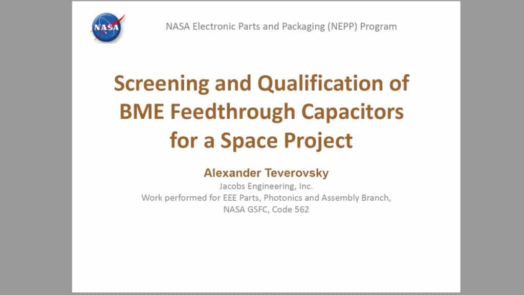
The part is a 10 nF BME X7R, size 0805 feedthrough capacitor rated to 50V and 1A DC input-output current. The specified insulation resistance is 1 Gohm and DC input-output resistance is 0.15 ohm. The evaluation tests included assessments of the capability of the parts to sustain high current pulses, thermal resistances, breakdown voltages, and leakage currents at high temperatures and voltages. To check the effect of high current pulses, the reversibility of voltage drop measurements was tested by increasing and decreasing current stress steps at steps of 0.5A and 0.1 sec. Fig. 1a shows that increasing currents up to 5A did not damage the part. Similar tests at steps of 0.75A up to 7.5 A showed that I-V characteristics remained linear up to 6A indicating DC resistance of 0.11 ohm (see Fig. 1b). As can be seen from Fig. 1A, at currents ~5 A the voltage rises with time, which is due to increasing temperature of the nickel conductors.

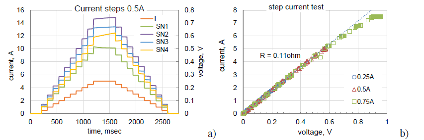
To assess the thermal run-away conditions, the parts were stressed by 12 steps of 0.1 sec pulses increasing with 1A increments (see Fig. 2a). Nickel features a relatively high temperature coefficient of resistance, 0.006 1/°C, which allows for estimations of the temperature rise based on resistance variations detected by voltage increase during the test. Results of these estimations show that a noticeable increase of temperature (~5.5 °C) occured at 7A and the thermal run-away condition when temperature sharply increased to more than 100 °C happened after 1 sec at 12A (Fig. 2a).
Using resistance of the Ni electrodes as a temperature sensor, the temperature rise was calculated for several capacitors soldered onto test PWB as shown in Fig.2b, and typical results of the constant voltage step stress tests are displayed in Fig. 2c. The characteristic time of the temperature rise is ~ 2 sec, and at a current of ~3.2A temperature rises up to ~ 28K.

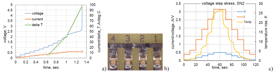
An infrared camera was used to get a more accurate assessments of the temperature rise at different levels of power dissipations. Results of these tests are shown in Fig. 3 and indicate a thermal resistance of the parts Rt = 29 ± 4 K/W. These values are about two times greater than the values of Rt calculated for chip capacitors with a few electrodes [4], but substantially lower than the values determined experimentally for chip tantalum capacitors (~ 100 K/W) [5].

At the rated conditions, I = 1A and RDC max = 0.15 ohm, the dissipated power will be 0.15W, and the possible temperature rise will not exceed 5 °C, which is acceptable for most applications.
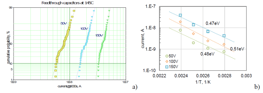
Leakage currents in the parts were measured in a wide range of temperatures, up to 145 °C and voltages, up to 150V. Distributions of leakage currents measured at 145 °C and different voltages and temperature dependencies of the currents are shown in Fig. 4. The distributions had no high leakage current tails thus indicating high quality of the product, and even at 150V and 145 °C leakage currents were below 0.1 mA. Both voltage and temperature increased current exponentially, which is consistent with the Schottky mechanism of conductivity [6]. The activation energy for the feedthrough capacitors was 0.49 ± 0.02 eV, which is consistent with the values for BME capacitors (0.4 to 0.6 eV).

Screening and Qualification
Screening and Qualification
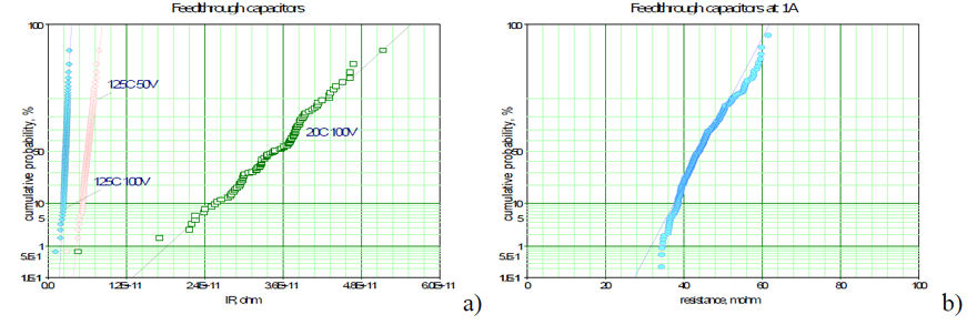
Three hundred samples were subjected to screening tests including visual examinations and measurements of all electrical characteristics including the through resistances that have been measured using a dynamic power SMU (Keysight N7973A) at high currents (1A). Visual inspections for workmanship defects and possible physical damages did not reveal any anomalies. All parts had electrical characteristics within the specified limits and analysis of distributions showed no out-of-family samples. Distributions of insulation resistances (IR) measured at room temperature and 125 °C are shown in Fig. 5a. Note that due to exponential increase of leakage currents, IR values are decreasing at higher voltages. Nevertheless, all samples exceeded substantially the specified limit of 1 Gohm not only at room temperature, but also at high temperatures and voltages exceeding the rated. Input-output DC resistances were within the specified requirements, R < 150 mΩ (see Fig. 5b).

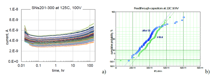
Burning-in was carried out for 300 samples at military conditions: 160hr at 125 °C and 2×VR. The leakage currents were monitored through the testing using 100kΩ current sense resistors. Typical results of BI testing are shown in Fig. 6a. No failures or anomalous behavior of currents was observed. The currents remained in the nanoampere range and the level of the current increase with time that is typical for BME capacitors was not significant.

One hundred forty of the screened samples were soldered onto test PWBs and used for qualification tests per the test flow shown in Fig.7. The tests were carried out using two subgroup of capacitors. The first one (80 samples) was used for temperature cycling (TC) followed by humidity testing. These tests did not result in any failures, and no excessive leakage currents that could have indicated the presence of cracks were detected during monitoring of currents in the humidity chamber at 10 V, 85% RH, and 85 °C (see Fig. 7b). Measurements of IR after humidity testing confirmed that insulation resistances of all parts were below the specified limit.

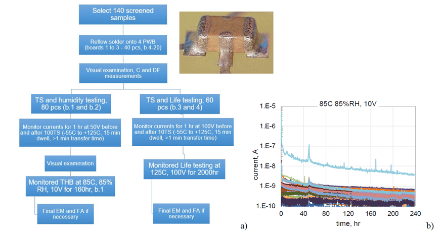

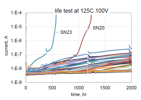
The second subgroup, 60 soldered samples, after 10 TC was used for monitored life testing that was also carried out at military conditions: 125 °C, 100V for 2000 hr. Variations of leakage currents with time of life testing are shown in Fig.8. For most samples, the current gradually increased with time from ~3 nA initially up to ~200 nA after 2000 hours. This behavior is typically attributed to the presence of oxygen vacancies that migrate under electric field in the bulk of capacitors and modulate the Schottky electron emission at the electrodes. Due to a relatively high activation energy of the process and the trend of leakage current to stabilize with time, this degradation does not pose a reliability risk.
Two samples, SN 23 and SN20 had substantially more significant increase in leakage currents and failed eventually after 570 hours and 1240 hours respectively. The failed samples were disconnected, so only 58 capacitors finished 2000-hour testing. IR values in parts that pass life testing were above 5E10 ohm at 50V and above 1E10 at 100V, which complies with the MIL-PRF-32535 requirements. The failed samples had shorts with resistances of 28k for SN20 and 2k for SN20. However, no defects were found during visual examinations. Both samples have been submitted for failure analysis.
Failure Analysis
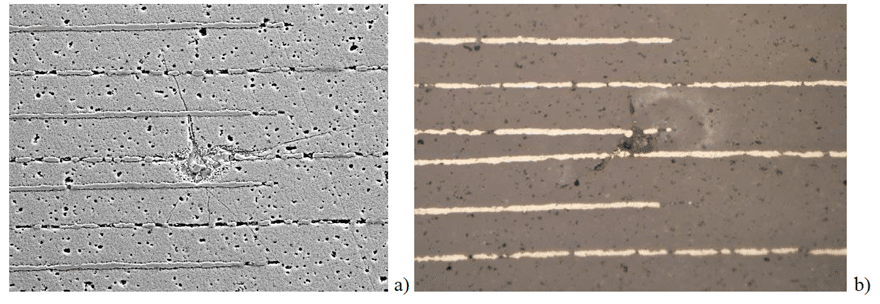
Acoustic microscopy and cross-sectioning were successfully used to locate and reveal damage in the failed samples. In both cases, the damage was due to a local breakdown that resulted in shorting electrodes by molted nickel (see Fig. 9). Both failure sites were associated with areas of thinning of the dielectric from 13 μm in normal areas down to 5-7 μm at the failed sites. Apparently, this thinning of the dielectric is a manufacturing defect that supposed to be screened out during burning-in of the parts. To get a better understanding of why these parts passed screening and what is the significance of these defects for application conditions, different groups of parts were tested at highly accelerated life test (HALT) conditions.

HALT and Discussion
HALT and Discussion
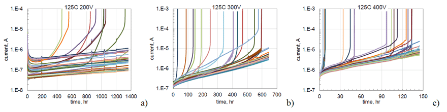
Leakage currents in three groups of the feedthrough capacitors with 40 samples each were monitored during HALT at 125 °C and voltages of 200, 300, and 400V. Results of these measurements are shown in Fig. 10. Failures of the parts were easily identified by increasing leakage currents above 1 mA that followed a period of a relatively smooth increasing of currents that lasted a few hundred hours at 200V, dozens of hours at 300V, and hours at 400V.

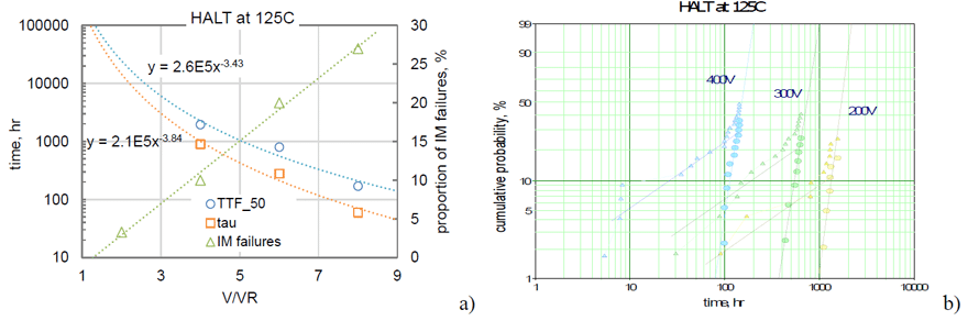
Parts that did not fail during HALT had also currents increasing with time. The intrinsic increase of leakage currents occurs exponentially with time and the rate of increase was consistent between different samples in the group. Variations of intrinsic currents with time can be described using a characteristic time of degradation t: I ~ exp(t/t). The characteristic time decreases substantially with voltage as shown in Fig. 11a, and following the Prokopowicz-Vaskas model, can be described with a power function, t ~ (V/VR)-m, where in our case m = 3.84.
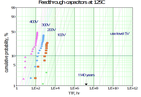
Fig. 11b shows distributions of times-to-failure (TTF) in Weibull coordinates during HALT at different voltages. The median times to failure (TTF50) are also plotted against the normalized test voltages in Fig.11.a. Similar to t, variations of TTF50 were approximated with a power function, TTF50 ~ (V/VR)-n, where n = 3.43. Close values of the exponents indicate that similar mechanisms might cause degradation and failures of the parts. Extrapolation to V/VR = 1 in both cases indicate times exceeding 20 years at 125 °C. Conservative estimations (Ea =0.7eV) show that reduction of temperature to 85 °C increases these times by a factor of 10.
The shape of distributions suggests the presence of infant mortality (IM) and wear-out (WO) failures. By treating these two groups of samples separately (competing failure modes), we can analyze distributions of IM and WO failures independently. The slopes of distributions (b) for WO failures (solid lines in Fig.11b) at all stress conditions was close and varied from 6.5 to 7.5, which is well within the criteria for WO failures, b > 1. Due to a wide spread of data, the accuracy of estimations of b for IM failures is poor, but assuming similar slopes for IM distributions at different stress voltages, these slopes were assessed as 0.7 as shown by dashed lines in Fig. 11b.
The interception point of the lines approximating WO and IM distributions (Fig. 11b) gives an assessment of the proportion of IM failures in the group, P(V), that depends on the stress voltage. This proportion increases from ~10% at 200V to 20% at 300V and 27% at 400V. Assuming that the failures observed during the standard life test condition (125 °C 100V) were also IM failures. P(100) = 3.3%. The value of P decreases linearly with voltage (see Fig. 11a) and might be well below 1% at the rated voltage. Considering that temperature has also a strong effect on the probability of IM failures, the risk of having these failures at operating conditions might be negligibly small. Apparently, the higher the level of stress, the larger proportion of IM parts can be revealed.

Analysis of the mechanisms of failures in BME ceramic capacitors shows that defect-related IM failures and WO failures are due to the same mechanism, migration of oxygen vacancies that is significantly accelerated at the defect areas such as local thinning of the dielectric [7]. In the first approximation, the same acceleration factors can be used for IM and WO failures and the probability of failures can be modeled using a general log-linear model that allows for presenting the characteristic time to failure, TTFchar in a form compliant with the Prokopowicz-Vaskas equation: TTFchar = A×V-n . Results of this modeling are shown in Fig.12 where the lines were calculated using maximum likelihood estimation (MLE) method as A = 1.4E13 hr, b = 1.14, and n = 4.12. The voltage acceleration constant, n, is in the range of values (from 3.9 to 8.7) determined for various X7R BME capacitors in [8]. Note, that the slopes of distributions in Fig.12 are substantially less than for WO failures shown in Fig.11b due to the inclusion of IM failures.
Based on this model, the probability of failures at the use conditions can be estimated (see Fig.12). For wear-out degradation, the most important parameter is the time to the failures’ inception, which can be defined as a time when 1% of failure occurs. For the life test conditions (125 °C, 100V), this time is ~ 400 hours, but for operating voltages (5V) it is 1.7E8 hours or 19,000 years. At 5V and 125 °C the inception of failures at 90% confidence, exceeds 1000 years. This indicates that failures detected at the military-level life test conditions will practically never happen at the use conditions. Conservative estimations show that the risk of failure for a 20 year mission at 5V is negligibly small, below 1E-7.
Modeling shows that the probability of failures at the BI conditions (160hr, 125 °C, 100V) is ~ 0.08%. This is in agreement with our experimental data showing no failures in 300 samples. Assessments based on the analysis of WO failures only, show that the time for the failure inception at 125 °C 100V exceeds 10,000 hours, which is far greater than the duration of the BI testing (160 hr). This means that the used BI conditions practically do not consume the life resource of the part and can be safely used for screening of the feedthrough capacitors.

A gradual increase of leakage currents before catastrophic failures as evident from Fig.8 and Fig.10 is consistent with the failure model suggested in [7]. According to this model, degradation of leakage currents occurs more rapidly in defect areas with thin dielectric due to increased electric field that intensifies migration of the positively charged oxygen vacancies, VO++, in the ceramic. Accumulation of the vacancies at the cathode reduces the barrier at the cathode-dielectric interface and increased current density exponentially. As a result, the temperature of the defect increases, which increases the current and creates a risk of the thermal run-away. A catastrophic failure happens when the hot spot temperature approaches melting points of ceramic or nickel (above 1000 °C). The probability of the run-away depends on the thermal resistance of the local area that decreases substantially with the size of defects, and on the availability of sufficient concentration of oxygen vacancies to reduce the barrier height.
Increasing temperature and voltage during HALT increases the probability of catastrophic failures caused by a defect substantially. However, this failure might never happen at normal operating conditions and the temperature of the defect can stabilize at a relatively low level. Results of HALT, where the larger proportion of IM failures indicating larger portion of defects in the parts that can be revealed at higher test voltages is in agreement with the model.
Results show that the existing system of qualifying parts for a space project by requiring that a certain number of samples pass life testing at 125 °C and two times rated voltage is not adequate not only for the automotive grade feedthrough capacitors, but in general, for advanced thin dielectric BME capacitors. The applicability of a given lot of capacitors for a specific space mission conditions should be based on adequate burning-in screening and assessments of the probability of failure during the mission. The latter can be done using a physics of failure approach, reliability modeling, and assessments of the acceleration factors using HALT.
Summary and Conclusion
Summary
Feedthrough BME 10nF size 0805 capacitor rated to 50V and 1A DC input-output current have been evaluated for high current capability and leakage currents in a wide range of temperatures. The thermal run-away when temperature sharply increased to more than 100 °C happens after 1 sec at 12A that provides sufficient margin compared to the rated conditions. The thermal resistance of the parts is Rt = 29 ± 4 °K/W, so at the rated conditions the possible temperature rise will not exceed 5 °C, which is acceptable for most applications. Distributions of leakage currents and breakdown voltages had no out-of-family samples indicating high quality of the product. Leakage currents even at 150V and 145 °C were below 0.1 mA and the activation energy was 0.49 ± 0.02 eV, which is consistent with the values for BME capacitors.
Screening of 300 samples showed that performance of the parts were well within the specification requirements. Monitored burning-in per MIL requirements (160 hr at 125 °C and 2×VR) did not result in failures or any anomalies in behavior of leakage currents indicating adequate quality control during manufacturing. Parameters of the capacitors after burning-in did not change substantially compared to the initial values indicating that BI conditions did not cause degradation of the dielectric.
No failures or any anomalies in behavior of 80 samples that after soldering onto PWBs were subjected to 100 TC between 125 to -55 °C was detected. After TC testing, the parts passed humidity testing when leakage currents were monitored at 85% RH and 85 °C for 240 hrs.
Two out of 60 capacitors reflow soldered onto test boards failed life testing at military-level conditions, 125 °C, 2VR, 2000hrs. Life testing did not result in any substantial variations in distributions of VBR and IR indicating the absence of the intrinsic degradation in the dielectric. The failures that happened after 570 hours and 1240 hours were due to a local thinning of the dielectric that resulted in accelerated degradation in the defect area.
HALT at 125 °C and stress voltages exceeding the rate voltage in 4, 6, and 8 times was used to assess voltage acceleration factors and the probability of failure at the use conditions. Based on conservative estimations, the risk of failure for a 20 year mission at 5V is negligibly small, below 1E-7.
Distributions of the times-to-failure during HALT indicate the presence of infant mortality and wear-out failures, and the proportion of the defect-related, IM failures increases at higher voltages. However, analysis of the physics of the degradation processes and estimations of the probability of failures show that IM failures that can be revealed at high voltages might never happen at normal operating conditions. Assessments based on the analysis of WO failures, show that the used BI conditions do not reduce the resource of the part and are adequate for screening of the feedthrough capacitors.
Analysis shows that in spite of the fact that military-level life test can result in failures of automotive-grade BME capacitors, the parts can operate reliably for a space mission. Using life testing as a quality (compliance) test might require relaxing stress conditions compared to the existing military-level requirements. Selection of adequate conditions following this approach is very expensive and difficult because it requires accumulation of substantial statistical data. A more practical approach is the assessment of the reliability for a given lot of parts for a specific application conditions based on the physics of failure, reliability modeling, and assessments of the acceleration factors using HALT. This approach might be especially effective for advanced COTS capacitors where WO failures became more critical and might limit the useful life of capacitors.
Acknowledgment
This work was sponsored by the NASA Electronic Parts and Packaging (NEPP) program. The author is thankful to Bruce Meinhold, SSAI ESES III Group Manager/SME, Parts, Packaging, Advanced Technologies, and Susana Douglas, NASA GSFC, Code 562 Parts Engineer for a review and discussions, and to the project PEs and manufacturers of capacitors for support and providing samples for this study.
References
[1] T. Zednicek, “Commercial versus COTS+ versus Qualified Passive Components in Space Applications,” presented at the EPCI e-Symposium, ESA/ESTEC, Noordwijk, The Netherlands, 2019. https://passive-components.eu/commercial-versus-cots-versus-qualified-passive-components-in-space-applications/
[2] NESC, “Recommendations on Use of Commercial-Off-The-Shelf (COTS) Electrical, Electronic, and Electromechanical (EEE) Parts for NASA Missions,” NASA Engineering and Safety Center NESC-RP-19-01490, 2020, https://www.nasa.gov/nesc/reports/
[3] D. Friedlander, “The use of COTS components in space: debunking 10 myths,” Intelligent aerospace, July, 5 2017 https://www.intelligent-aerospace.com/articles/2017/10/electrical-electronic-and-electromechanical-cots-components-in-space-penalizing-policy.html
[4] F. M. Schabauer and R. Blumkin, “Thermal resistance, power dissipation and current rating for ceramic and porcelain multilayer capacitors.” American Technical Ceramics: Theta-J Associates, 1981, http://www.theta-j.com/pdf/ce/articles/atc_article-Thermal_Resistance.pdf.
[5] E. K. Reed, “Tantalum chip capacitor reliability in high surge and ripple current applications,” in 44th. Electronic Components and Technology Conference, 1994, 1-4 May 1994, pp. 861-868.
[6] A. Teverovsky, “Leakage Currents in Low-Voltage PME and BME Ceramic Capacitors,” presented at the 7th International Conference on Electroceramics (ICE2015), Penn State Conference Center, State College PA, USA, 2015. https://nepp.nasa.gov/
[7] A. Teverovsky, “Failure models for low-voltage BME ceramic capacitors with defects,” in 2017 IEEE International Reliability Physics Symposium (IRPS), 2017, 2-6 April 2017, pp. 6C-5.1-6C-5.8.
[8] D. Liu and M. Sampson, “Reliability Evaluation of Base-Metal-Electrode Multilayer Ceramic Capacitors for Potential Space Applications,” in CARTS USA, Jacksonville, Fl, 2011, March 28-31.

