


The article explains construction, manufacturing, application and features of ceramic capacitors.
Key Takeaways: MLCC and Ceramic Capacitors
- Ceramic Capacitors Dominate the Market
- MLCCs (Multilayer Ceramic Capacitors) are the most widely used capacitor type due to miniaturization, low ESR, and high capacitance density.
- SLCC vs. MLCC Construction
- SLCCs are simple, low-cost, and used in RF/high-voltage applications. MLCCs stack hundreds of layers, enabling high CV and extreme downsizing (0201, 008004 sizes).
- Dielectric Classes Define Performance
- Class 1 (NP0/COG) offers stability and low losses for resonant circuits. Class 2 (X7R, Z5U) provides higher capacitance density but with variation due to temperature, voltage, and aging.
- Manufacturing Evolution
- Industry shifted from Precious Metal Electrodes (PME) to Base Metal Electrodes (BME) like nickel and copper, reducing costs and enabling higher CV designs.
- Miniaturization Enables Modern Electronics
- Case sizes shrank from 0805 in 1995 to 0201 and 008004 today, powering smartphones, automotive ECUs, and compact devices.
- Reliability and Failure Modes
- MLCCs face risks like micro-cracks, delamination, and capacitance loss under DC bias. Flexible terminations improve reliability in automotive and aerospace applications.
- Specialized Variants
- High-voltage MLCCs, thin-film RF capacitors, low-ESL designs, and leaded/discoidal types address niche requirements from power electronics to EMI filtering.
- Performance Trade-offs
- Higher capacitance requires thinner dielectrics, increasing failure risk. Class 2 ceramics suffer from aging, DC bias effects, and piezoelectric noise.
- Industry Relevance
- MLCCs are indispensable in consumer electronics, automotive, aerospace, and energy systems, balancing cost, performance, and reliability.
Ceramic dielectric electrostatic capacitors are dominating capacitor market in number of fields:
- Largest volume capacitor technology (by far)
- Largest value capacitor technology
- Smallest dimension discrete components among all passives
- High flexibility of design to meet specific requirements such as low ESL / high frequency operation
- Strong presence in both low voltage, low power and high voltage, high power applications
despite all the above benefits there are some limitations of the technology that has to be understand for the correct use and design-in. In the following chapters we will also discuss two major groups of ceramic dielectric materials:
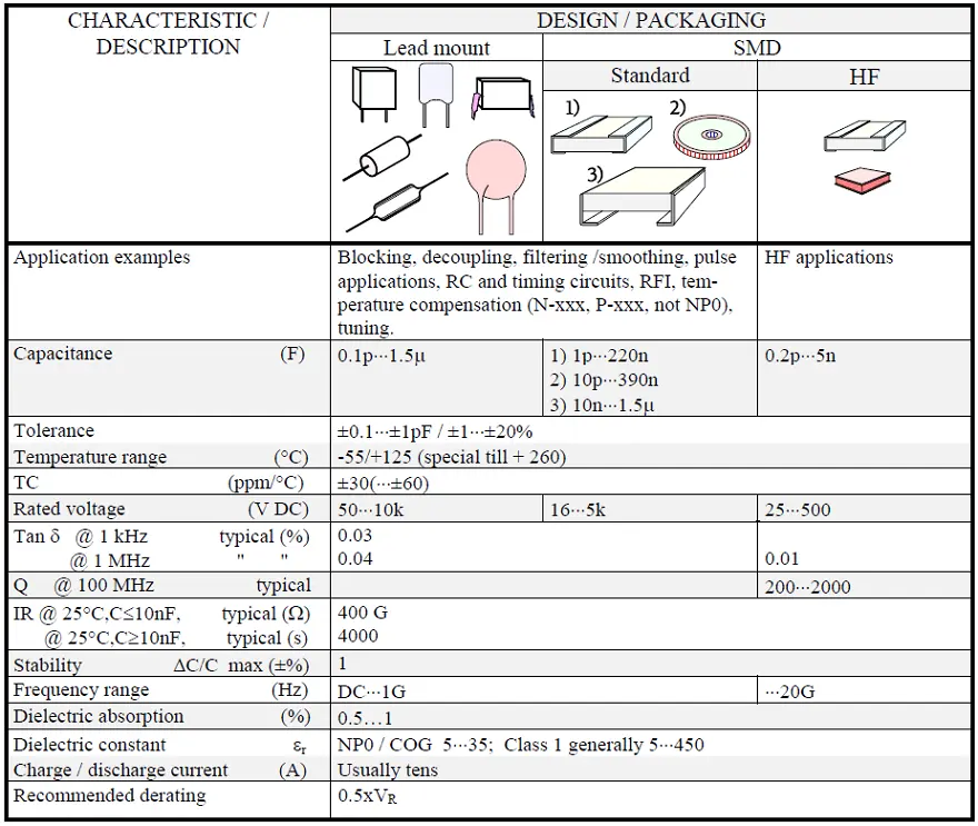
Introduction to Ceramic Capacitors
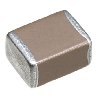
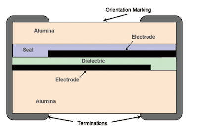
The basic construction types include simple – single layer SLCC ceramic capacitors and major types made by stacking technology – MLCC multilayer ceramic capacitors.
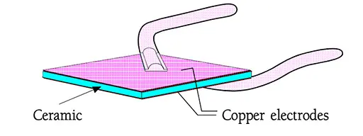
Single layer ceramic capacitor SLCC
- simple construction
- low cost technology
- lower CV
- higher ESR
- wide voltage range
- high voltage, high power applications
- RF/microwave applications
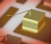
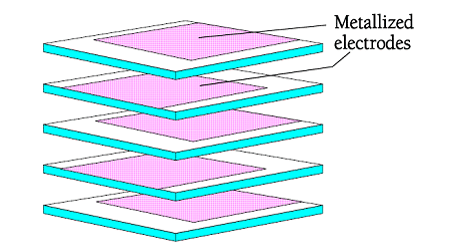
Multilayer MLCC ceramic capacitors
- mass volume
- miniaturization
- low ESR
- high CV
- flexible technology
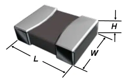
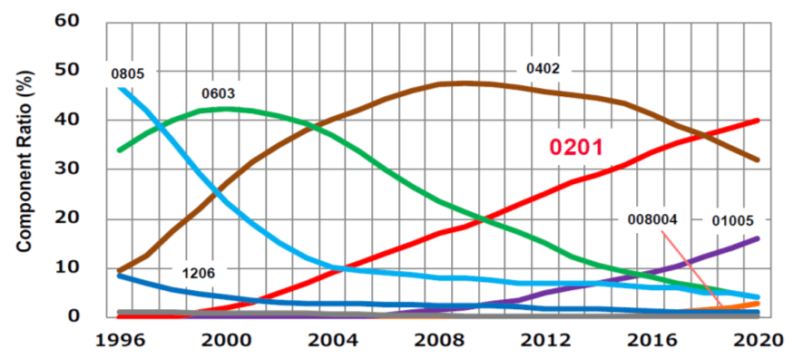
MLCCs chips are by far the leading downsizing and miniaturization technology among passive components. Chart bellow is illustrating shift of the case size mix in MLCCs. While the most popular case size in 1995 was 0805, 0603 in 2000, 0402 in 2009, the most often used case size since 2018 is 0201 that is a capacitor in dimensions 0.6×0.3×0.3mm. The smallest so far MLCC in mass manufacturing is 008004 case introduced to volume production in 2019 with dimensions as small as 0.2×0.1×0.1 mm.
MLCC Case Size Standards
MLCC requirements fall under EIA-198. Their standardized size and shape offerings are a reflection of American EIA standards, often represented using Imperial measurements (e.g., inches) rather than Metric. When reading a specifications chart, like Figure 1, EIA dimension codes correspond with the dimensions of the MLCC itself. For example, a rectangular chip with the dimensions 0.08 inches in length by 0.05 inches in width is coded as “0805.” Looking at the chart, you’ll notice International Electrotechnical Commission/ European Standard (IEC/EN) codes too. The Joint Electron Device Engineering Council (JEDEC) established this set of specifications to represent the Metric system. See Figure 1. below with EIA inch and IEC/EN metric dimension and codes.
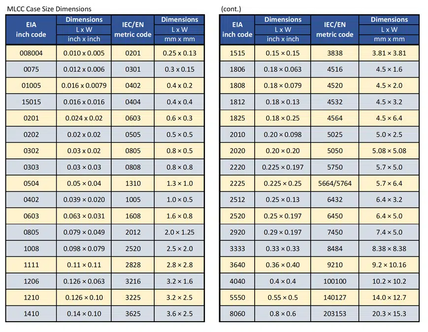
more information about – read the post: MLCC Case Sizes Standards Explained
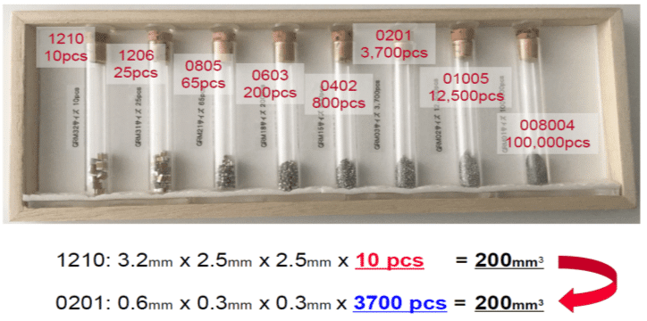
The enormous volumetric downsizing is illustrated in Figure 1. and 2. bellow – about the same volume taken by 10 pieces of 1210 case size is occupied by 100 000 pieces of 008004 capacitors !
Ceramic Dielectric Classifications
The different ceramic dielectric materials used for ceramic capacitors with linear (paraelectric), ferroelectric, relaxor-ferroelectic or anti-ferroelectric behaviour (Figure 3.), influences the electrical characteristics of the capacitors. Using mixtures of linear substances mostly based on titanium dioxide results in very stable and linear behavior of the capacitance value within a specified temperature range and low losses at high frequencies. But these mixtures have a relatively low permittivity so that the capacitance values of these capacitors are relatively small.
Specific group of materials are anti-ferroelectric dielectrics. In opposite to ferroelectrics, where permittivity decrease with applied voltage, permittivity of anti-ferroelectics is low at low voltage and increase with electric field / appled voltage. These materials can be used to achieve high CV, high capacitance at high voltage applications such as energy generation or EV/HEV vehicles in automotive industry. See Figure 3. bellow for comparison of polarisation curves between linear dielectrics (class 1), ferroelectrics (class 2) and anti-ferroelectric materials. We will discuss more in class 2. ceramic capacitors chapter.
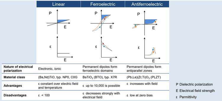
Higher capacitance values for ceramic capacitors can be attained by using mixtures of ferroelectric materials like barium titanate together with specific oxides. These dielectric materials have much higher permittivities, but at the same time their capacitance value are more or less nonlinear over the temperature range, and losses at high frequencies are much higher. These different electrical characteristics of ceramic capacitors requires to group them into “application classes”.
The definitions of the application classes given in the two standards are different. The following table shows the different definitions of the application classes for ceramic capacitors:
| Definition regarding to IEC/EN 60384-1 and IEC/EN 60384-8/9/21/22 | Definition regarding to EIA RS-198 |
|---|---|
| Class 1 ceramic capacitors offer high stability and low losses for resonant circuit applications. | Class I (or written class 1) ceramic capacitors offer high stability and low losses for resonant circuit application |
| Class 2 ceramic capacitors offer high volumetric efficiency for smoothing, by-pass, coupling and decoupling applications | Class II (or written class 2) ceramic capacitors offer high volumetric efficiency with change of capacitance lower than −15% to +15% and a temperature range greater than −55 °C to +125 °C, for smoothing, by-pass, coupling and decoupling applications |
| Class 3 ceramic capacitors are barrier layer capacitors which are not standardized anymore | Class III (or written class 3) ceramic capacitors offer higher volumetric efficiency than EIA class II and typical change of capacitance by −22% to +56% over a lower temperature range of 10 °C to 55 °C. They can be substituted with EIA class 2- Y5U/Y5V or Z5U/Z5V capacitors |
| – | Class IV (or written class 4) ceramic capacitors are barrier layer capacitors which are not standardized anymore |
The most common Class I. (low loss, low capacitance density) and Class II. (high loss, high capacitance density) materials are discussed in next chapters.
Construction & Manufacturing Process
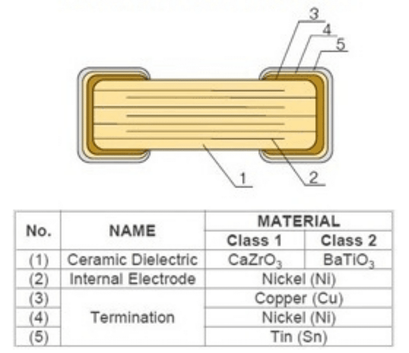
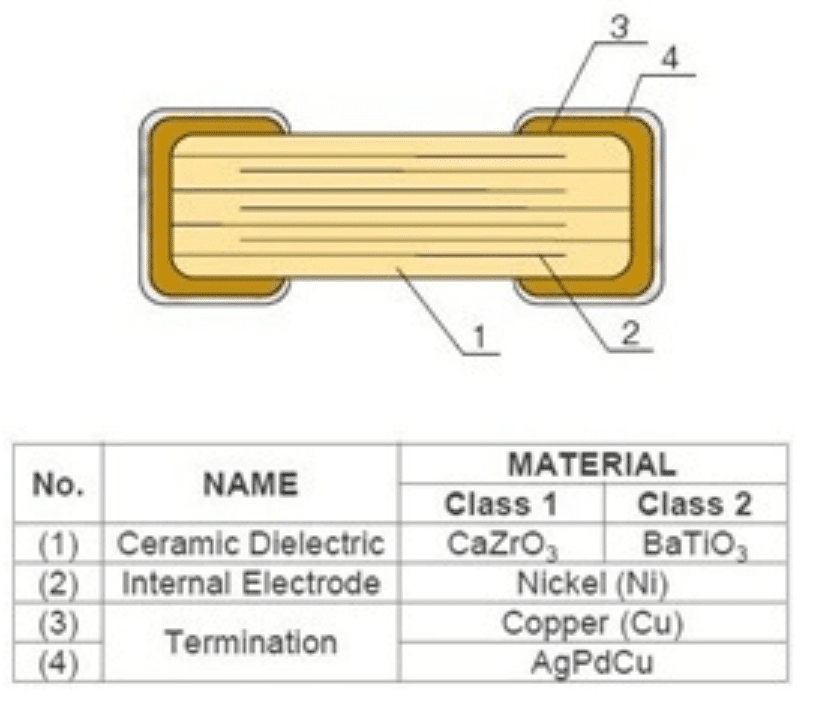
The capacitors consist, as the name tells us, of some kind of ceramic. The manufacturing process starts with a finely grounded ceramic powder mixed to an emulsion of solvents and resin binders. In the first manufacturing step the emulsion then is dried to a soft film and screen printed with an electrode paste, historically it was a compound of palladium or silver and palladium + binding agents. Due to the high cost of palladium this termination style was replaced by metals like copper and nickel, so called base metal electrodes (BME) that is a majority of todays MLCC designs.
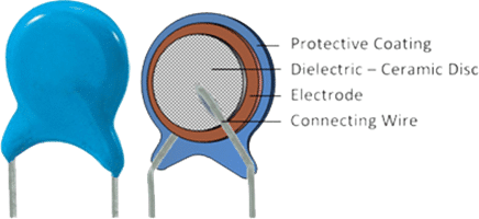
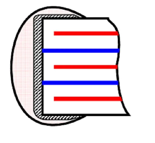
So called tube capacitors are extruded out of a nozzle and are covered with an electrode paste on the inside and the outside before it’s sintered to its definite material structure. In the same way the Single Layer Ceramic Capacitor (SLCC or just SLC) consists of one dielectric layer. The ceramic is covered with an adhesive layer of, for example, chrome nickel as a base for copper electrodes. On the electrodes leads are soldered as shown in the principle Figure 5., before the component is encapsulated in lacquer or epoxy.
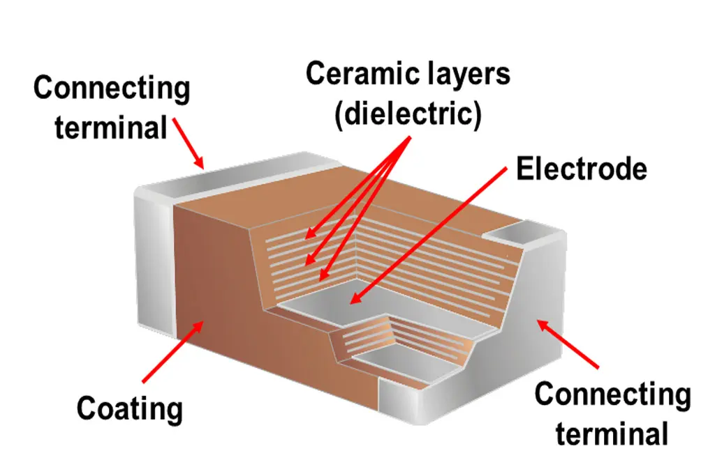
The most common design of a ceramic capacitor is the multi layer construction where the capacitor elements are stacked, so called MLCC (Multi Layer Ceramic Capacitor). The number of layers has to be limited for reasons of the manufacturing technique. The upper limit amounts at present to over 1000. Besides economical reasons come into play. On larger case sizes, stacking operation becomes less productive and raise the price steeply at higher capacitance values. The lowest capacitance values are achieved by only two layers, often separated by double ceramic layers.
MLCC Manufacturing Process
In the conventional so called dry method the ceramic emulsion is dried on a conveyor belt before it is separated from the supporting bed. After it is cut into “primary sheets” that are screen printed with electrode paste for a large number of chips. These primary sheets then are stacked in an accurate steel frame and pressed to a solid piece in order to make it possible to cut out the separate chips from the stack with the electrodes in alternating positions.
In the latest variant of this method one utilizes a conveyor film for the ceramic emulsion and has thus succeeded in reducing the dielectric thickness to 3 μm (0.1 mil). Here the quality implies manufacture in extremely “clean rooms”, i.e. in rooms with filtered air and control of the number and size of particles.
Before the variant with a conveyor film was used in the dry method, the so called wet method was becoming more and more common. There the stage with handling of “primary sheets” is skipped by letting the emulsion dry in “primary sheet frames”. In combination with better milling methods for the ceramic powder and a higher material purity the wet method makes it possible with thinner dielectrics without a growing failure rate.
An MLCC consists of a number of individual capacitors stacked together in parallel and contacted via the terminal surfaces. The starting material for all MLCC chips is a mixture of finely ground granules of raw materials, modified by accurately determined additives. These powdered materials are mixed homogeneously. The composition of the mixture and the size of the powder particles, as small as 10 nm, reflect the manufacturer’s expertise.
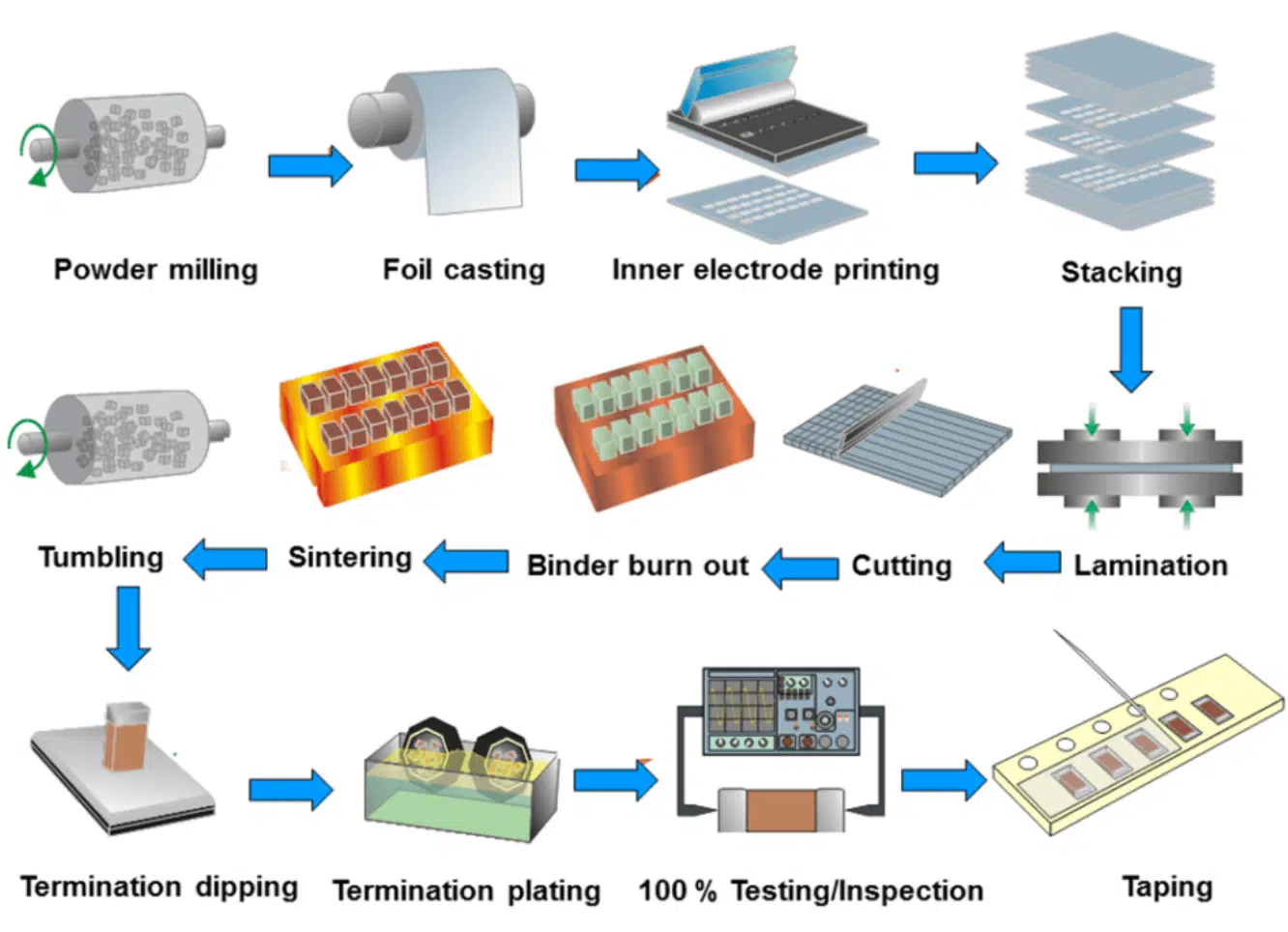
A thin ceramic foil is cast from a suspension of the powder with a suitable binder. This foil is rolled up for transport. Unrolled again, it is cut into equal-sized sheets, which are screen printed with a metal paste. These sheets become the electrodes. In an automated process, these sheets are stacked in the required number of layers and solidified by pressure. Besides the relative permittivity, the size and number of layers determines the later capacitance value. The electrodes are stacked in an alternating arrangement slightly offset from the adjoining layers so that they each can later be connected on the offset side, one left, one right. The layered stack is pressed and then cut into individual components. High mechanical precision is required, for example, to produce a 500 or more layer stack of size “0201” (0.5 mm × 0.3 mm).
After cutting, the binder is burnt out of the stack. This is followed by sintering at temperatures between 1,200 and 1,450 °C producing the final, mainly crystalline, structure. This burning process creates the desired dielectric properties. Burning is followed by cleaning and then metallization of both end surfaces. Through the metallization, the ends and the inner electrodes are connected in parallel and the capacitor gets its terminals. Finally a 100% measuring of the electrical values will be done and the taping for automated processing in a manufacturing device are performed.
There are two basic termination structures – BME Base Metal Electrodes based on copper and nickel metals and PME Precious Metal Electrodes based on silver palladium metals. The original technologies were using mostly PME structure but palladium high prices pushed industry to look for alternatives. Advantage of PME has been its TCE compatibility with the glass dielectric and thus lower stress during firing process. However, BME is now the dominating structure and subjected to the latest developement, thus higher CV capacitors are available in BME configuration, while PME is used in mission critical applications such as space or defense.
The separate cut loose chips are subjected to a first heat treatment (burn-out) where the organic binding agents – also those being part of the electrode paste – are gasified and diffuse through the not yet sintered ceramic. If this process is forced too fast gas bubbles are formed that will separate electrodes and ceramics and results in so called delaminations (Figure 10.).
The risk with a delamination also increases with the number of layers. Primarily it depends on the quantity of electrode metal in the ceramic and the differences in TCE (coefficient of expansion) of these materials. At the maximum of capacitance in a certain chip size a delamination is nearly unavoidable.
Now a delamination may not be that catastrophic that we fear. If the capacitor is not subjected to extreme humidity that might diffuse into the cavities and the soldering is executed without any unsymmetrical heat conduction that may cause cracks in the ceramic we will never become aware of any delaminations (unless we deal with high voltage capacitors where the corona effect may be dangerous). It’s the authors opinion that only soldering with a soldering iron will cause such temperature gradients that the ceramic may crack. There are, however, other reasons why it may be advisable to avoid the highest capacitance values.
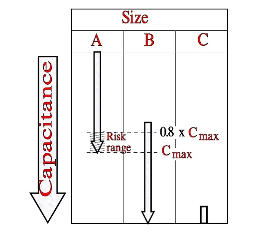
The dielectric thickness, the number of electrode layers and the active capacitive area determine the capacitance in a certain chip size. The thickness is varied by using one or several layers. But when we on the way towards higher capacitances pass from two to one layer the risk of short-circuit failures increases. It will, of course, be at maximum when we pack the chip with the maximum number of layers. At the same time the risk of delamination increases. A practical limit where it may be advisable to avoid this twofold risk range by a size exchange is approximately 20% below the usually starts overlapping in next chip size (Figure 11. left).
If the component operates at high electric field strengths or in severe mechanical acceleration or chock environments we should in any case avoid maximum capacitance values in that size class, i.e. reduce the capacitance or increase the mechanical size.
We can also buy “high-rel” components, for example according to MIL-C-123 that specifies limits for the delamination extent and states methods for X-ray diagnosis. The price, however, will be approximately 20 times higher than that of a conventional standard component and the success with the X-ray check is debatable. Other methods with ultrasonics are developed but the result is many times difficult to interpret. Besides such equipments are expensive. In conclusion only “space” and other “high rel” applications motivate the price we must pay for the increase in quality.
The burn-out process shouldn’t be forced too fast because of provoked delamination. On the other hand it may not last too long. Then impermissible much of the palladium content of the electrode paste will oxidize. In other words the time-temperature profile must be kept at an optimum level for the ceramic and electrode material.
After the burn-out process follows the considerably faster sintering of ceramic and electrode materials. Also here check of the time-temperature profile is extremely vital, not least the cooling time if we shall avoid micro-cracks in the ceramic.
After the sintering terminations are applied which consist of
- farthest BME or Ag/Pd in good adhesion to the ceramic, 15…40 μm (0.6…1.6 mils)
- possibly a barrier layer (Ni) that will prevent silver from dissolving into the solder, 1…3 μm (0.04…0.1 mil) and
- farthest out Sn, 3…10 μm (0.1…0.4 mil) or solder, 10…100 μm (0.4…4 mils)
If the inner electrodes consist of nickel or copper compatible termination materials have to be utilized. For that reason nickel or copper based compounds are developed for outer terminations. They have a low migration and need only to be covered with a solderable alloy.
Electro-plating of tin as the outermost layer gives an evenly thick layer also on edges and corners. But because of a perpendicular orientation of the tin crystals against the surface they are leaving access to oxidizing oxygen if the tin layer is too thin. Therefore it should rather be 10 than 3 μm thick (0.4 mils rather than 0.1 mil). Hot or dip tinning creates a very tight layer but with an uneven thickness. The covering on the corners becomes thin.
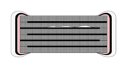
Flexible soft termination
Fail Safe Multilayer Ceramic Capacitors (MLCCs)
Multilayer ceramic capacitors are highly susceptible to mechanical cracking due to their brittle nature. It is necessary for circuit board manufacturers to ensure that their board handling techniques do not expose boards to excessive bending (board flex) during manufacturing and operation. Some of the processes that can expose boards to excessive bending include mounting in assembling and depanelization. Use of unsupported input/output edge connectors and pick-and-place equipment can also cause excessive bending.
Standard MLCCs have no crack protection and they are normally used for non-critical applications.
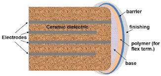
Soft termination (Flexiterm, Flexcrack etc … trade names) are based on principal to introduce a soft, conductive layer (usually conductive polymer) to the MLCC terminals that absorb mechanical stress. See figure on right.
These capacitors can withstand up to 2-5mm of board flexure without internal cracks. Beyond 5mm, capacitor will generally fail “open” and thus this style is the preferred solution today for automotive and higher reliability applications.
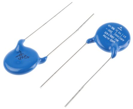
High Voltage SMT Ceramic Capacitors
Surface mount high voltage multilayer ceramic capacitors (HV MLCCs) appear to be pretty much identical to standard configuration MLCCs. They have the same basic form, fit and function, but there are several key differences.
Typically, as a matter of definition, high voltage MLCCs have rated voltages that are greater than or equal to 200VDC. High voltage MLCCs are typically available in EIA size from 0603 to 2225 or larger (metric 1608 to 5664) with voltage ratings from 200V to 5,000V or more. Smaller case high voltage MLCCs typically have lower maximum rated voltages (VRated) as the external terminals tend to be closer to each other in comparison to larger case high voltage MLCCs.
High voltage MLCCs are generally available with Class 1 (C0G) or Class 2 (e.g., Ferroelectric X7R) ceramic dielectrics with tolerances that are as good as +/-5% or better, to as wide as +/-20% or higher. Because of the generally thicker dielectric thicknesses used in the design and potentially the “cascade” or “floating electrode” type designs used, the maximum capacitance values available are significantly lower than standard MLCCs.
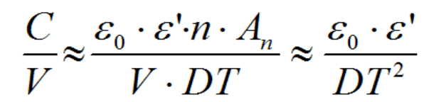
HVMLCCs appear similar to standard configuration MLCCs. It seems that it should be straight forward to design an HVMLCC of a given voltage rating; just keep increasing the dielectric thickness (DT) to enable the voltage rating desired as you would with a standard configuration MLCC. The rate of increase in DT used is typically about 200 to 250 Volts per thousandth of an inch (V/mil, or ~7.8 to 10 V/μm).
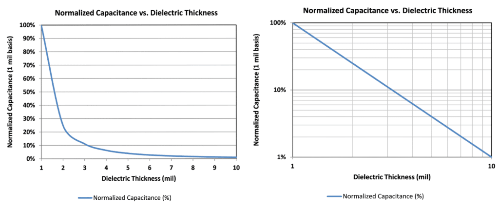
There is a penalty in capacitance per unit volume (C/V) using this approach to increasing rated voltage, as it requires increasing DT. The penalty in C/V is proportional to DT-2 following the relationship:
However, above ~1,500V, it gets more complicated than that. An example of the resulting penalty to C/V is illustrated in Figure below. As voltage rating is increased, DT must increase to the expense of C/V in a manner that is linear for the log-log relationship demonstrated on the right, where C/V is reduced 2 decade values for every one decade value increase in DT. Thus, as rated voltage is increased, capacitance per unit volume is reduced at a fairly dramatic rate.
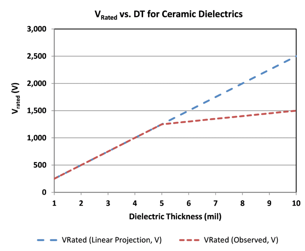
The above penalty in C/V as voltage rating is increased is not the only factor to consider however as the above as-sumes that a constant rate of increase in DT is appropriate to achieve increased voltage rating. While this is true, typically to ~1,000 to ~1,500VRated ceramic dielectrics tend deviate from that rate as VRated is increased above ~1,000 to ~1,500V, resulting in a different VRated vs. dielectric thickness relationship that is of lower slope. A hypo-thetical example of this is given in Figure below.
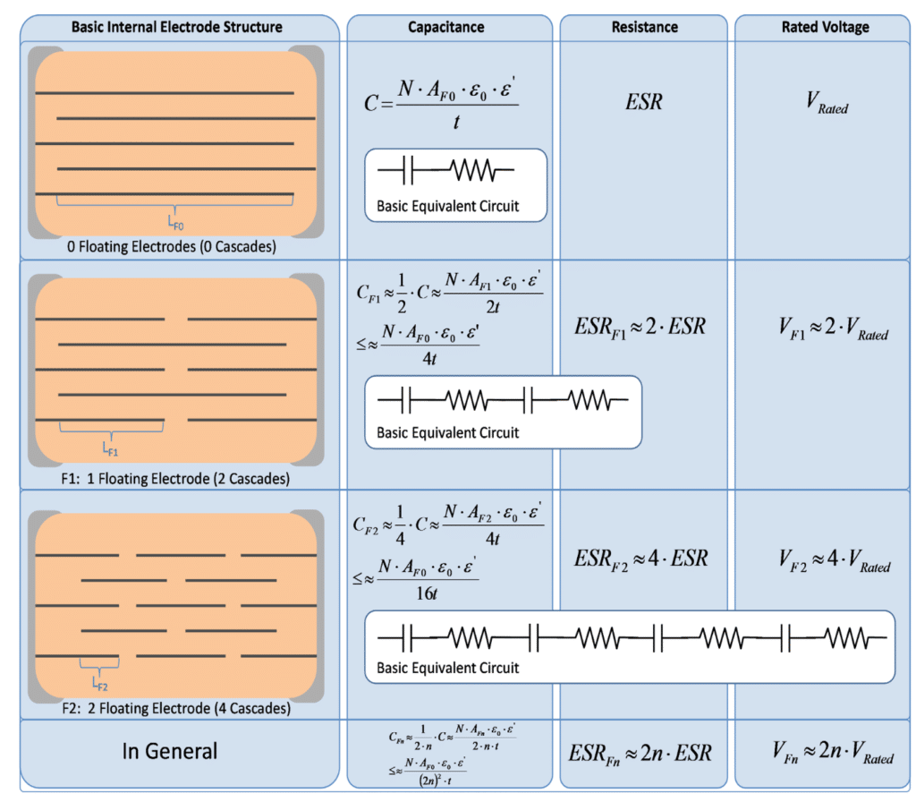
We can use floated electrodes (FE) or cascade electrode MLCCs to increase VRated with relatively minimized impact on C/V as compared to standard configuration MLCCs at lower voltages (i.e., <~1,000V to ~1,500V). As each FE has an additional margin area associated with it, the impact of additional margins on C/V in small case MLCCs (typically EIA 0603 and 0805) may be prohibitive, but for larger MLCCs (e.g., EIA 1206 to 2225) the impact is acceptable to relatively small.
As in Figure 16. below, C/V decreases commensurate with (1/2n2), where n is the number of FEs within the design. VRated also increases with 2n as does ESR. The effect on ESR is largely compensated for however, as the two or more internal capacitors typically have more electrodes in each internal capacitor stack (N), thereby reducing ESR within each capacitor in series, and since the aspect ratio of said electrodes within each of the internal capacitors in series has relatively wide and short electrodes, which results in further decreased ESR. These two factors work together to reduce ESR such that the projected ESR increase is typically negligible, and may even be reduced in comparison to standard configuration MLCCs of similar VRated.
Other Construction Types
RF Thin Film Ceramic Capacitors
Thin-film ceramic capacitors are using a single-layer low loss ceramic dielectric packaged as a multilayer ceramic capacitor (MLCC) – see figure below. Its advantage is in very tight capacitance tolerance (even low batch to batch variation) and a single resonant point response. Thus such design are ideal for RF and microwave filter designs.
A thin-film capacitor has an extremely repeatable frequency response compared to MLCCs.It is also important to realize the limitations of thin-film capacitors used as band-reject filters. Since thin-film capacitors are typically only available in low capacitance values they are limited to relatively high-frequency band-reject filter designs. If dealing with low frequency designs, other filter methods must be utilized typically using high-Q multilayer RF capacitors.
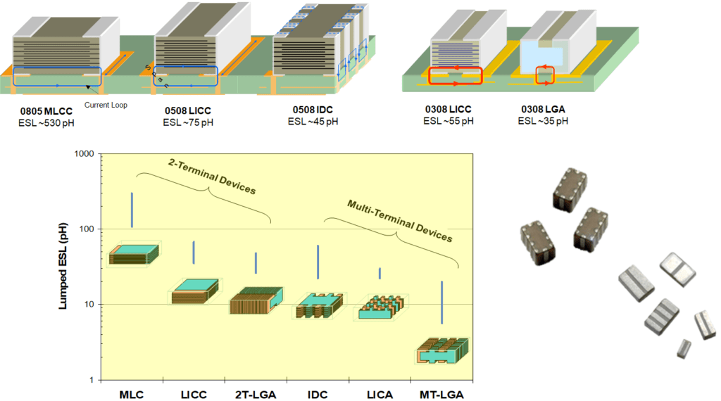
Low ESL designs
One of key MLCC stacking technology advantage is its flexibility in electrode / dielectric layers layout. This allows high customization level to match the technology with specific application field requirements. Low ESL, high frequency coupling is more and more important with the latest generation of processors. The following figure is illustrating possible design configuration to reduce ECL and enable higher frequency operation.
Lead mount MLCC
Lead mount components are supplied with leads. It can be encapsulated or stacked together by supported J-lead terminations, as in the following Figure 19.
The purpose of leaded MLCCs is not only in enabling of the technology for through hole assembly but in most cases reduce mechanical stress and risk of cracking at larger case sizes. This is commonly used in high rel industry or automotive to accommodate larger capacitance values while keeping high vibration robustness.
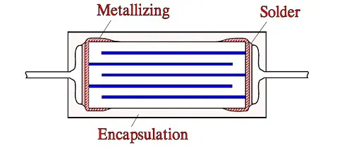
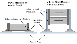
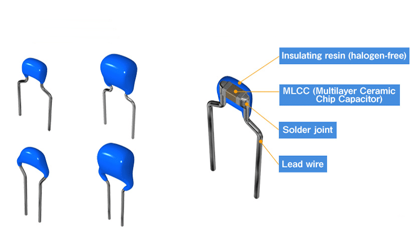

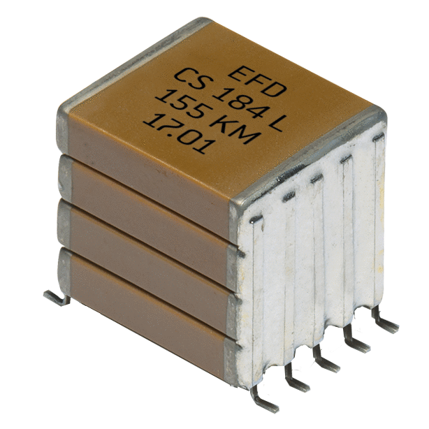
Figure 19. encapsulated, leaded stucked MLCC ceramic capacitors
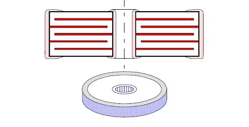
Discoidal
In filters and connectors another chip variant occurs, the concentric one called discoidal that are often used as a feedthrough capacitors.

Failure modes
Already during the construction report we have touched on some of the failure modes that may appear in ceramic capacitors. Probably the most common one in MLCCs is short circuiting at low voltage in high impedance circuits. It appears as micro-cracks in the ceramic. Under the influence of moisture and a polarizing voltage an electrolytic material transportation from one electrode to the other easily takes place. We call it “ionic migration”.
We get a short-circuit that to its character resembles the one that may occur in carbon contaminated self-healing sites in plastic film capacitors. Similarly the conductive path is extremely thin and is easily burnt away if the voltage exceeds certain minimum values. Should it on the other hand be too high we get a flash-over in the crack and this is hardly better.
It is well known that parts manufactured in older technologies had an increasing failure rate that started when the dielectric became thinner than 20…25 μm (» 0.8…1 mil). Even if some manufacturer’s technological progress has made the quality of thin dielectrics much better we still have to be cautious. The failure type is batch bound and manufacture dependent which among other things is connected with the sensitivity to dust and particles in the air.
Dielectric layers thinner than 50 μm (2 mils) require manufacture in clean rooms, i.e. rooms with filtered air and controlled number and size of particles. In other words knowledge about good manufacturers is a must. Certainly there are different methods to trace suspicious batches. In the so called “85/85 test” according to MIL-C-123 the capacitors are exposed to 85% RH at +85°C and maximum 1.5 V DC in series with 100 kΩ for at least 240 hrs. But the efficiency of this test is not one-hundred-per-cent.
Another failure that above all strikes the common SMD components is bad solderability and silver leaching in more severe soldering processes. In order to meet the solderability problem one ought to
- specify and check packaging method and component age and check the solderability in a wetting balance, at the relevant soldering temperature.
Hence storage of chips with their exposed terminations should be done in a protected environment. Above all we should be on our guard for cardboard boxes because they may have a sulfur content which will cover silver alloys with a sulfide layer that destroys the solderability.
The leaching problem can be met with requirements for a barrier layer / nickel barrier. But a general requirement may not be enough. The freedom of pores in the nickel layer and its thickness are important. Besides also here knowledge about the manufacturers is necessary.
There are many pitfalls in the form of poor cleaning from plating bath residues, negligence with the oxidation protection of the nickel layer etc. Finally the soldering process might be quite unsuitable for nickel barrier designs. The streaming solder from the wave soldering rapidly conveys heat to the component surfaces and especially to the hard, fast-wetting nickel barrier. Long before the ceramic body has got warm the nickel layer has reacted with its thermal expansion.
In chips larger than 1210 this leads to risk of cracks in the ceramic, inside the nickel barrier, especially if the layer is relatively thick. Therefore many leading manufacturers make larger sizes without any nickel barrier. But if we from serious manufacturers can find larger sizes with nickel barrier and they are not exposed to wave soldering but to the slower, more lenient processes like, for example, vapor phase, IR or hot air then chip sizes up to 2220 should be possible to use without any risk. Still larger sizes should have some kind of flexible terminals.
Ceramic Capacitors Class 1
Capacitors Class 1 are manufactured using low loss linear paraelectric ceramic dielectric materials with low temperature coefficients between +100 and –1500 ppm/°C. NP0 or COG (0 ± 30 ppm/°C) types are predominant over all remaining Class 1 variants.
To the Class 1 ceramics we also count porcelain that above all is found in certain HF chips.
General comments to Class 1
The type is characterized by small losses, high IR, high stability, linear and moderate TCs between +100 and – 1500 ppm/°C and an εr between 5 and 450. The tolerances range down to ±1%. Capacitances lower than 10 pF are difficult to produce to a percentage accuracy. The tolerances are rather stated in absolute values: ±0.1pF, ±0.25pF, ±0.5pF and ±1pF.
At construction and failure analysis you may sometimes find a pit in the ceramic of Class 1 capacitors. It may extend through all layers and is filled with some inert compound, often glaze. It is a so called trim pit where part of the electrode surface is blasted away in order to match the capacitance value towards finer tolerances, for example 1 or 2%.
The ceramic mass shrinks namely strongly during the sintering – approximately 15% – and this may cause the capacitance distribution to get so askew that it will be necessary to adjust it by trimming. The trim pits are harmless provided the filling compound don’t contain any blisters at the edge to adjacent layers.
The small losses in Class 1 ceramics do not correspond to a similarly low dielectric absorption. On the contrary it is relatively high, approximately 0.5…1%.
The dielectric consists either by one layer – as a tube or in a plane shape, SLC from Single Layer Ceramics, or by several layers in stacked form, MLC from Multi Layer Ceramics. In MLCs the capacitance range is determined by the number of layers. At minimum it consists of one layer and at maximum it is limited by the manufacturing technique and for economical reasons. The noble metal AgPd paste of the electrodes is expensive, mostly used BME is a cheaper variant.
The temperature coefficient often is denoted by N(egative) or P(ositive) followed by the value in ppm/°C. Here some examples where we within brackets mention also the corresponding EIA designation:
- P100 = +100±30ppm/°C; (EIA = M7G)
- NP0 = 0±30ppm/°C; (EIA = COG)
- N150 = -150±30ppm/°C; (EIA=P2G)
- N1500= -1500±250ppm/°C; (EIA=P3K).
US MIL specifications have other designations.
In diagrams and tables we henceforth confine ourselves to the predominant NP0/COG ceramic.
HF chips
When the frequency raises to some hundred MHz conventional ceramics in MLC design starts reacting with high and exponentially increasing losses. We come a step on the way by modifying the ceramic. By passing to porcelain (εr = 12…15), which we include under the concept ceramics Class 1, the losses decreases sharply. Another way to reduce the HF losses is by passing to a single layer design, SLC, and moreover introduce thin film electrodes in gold (Au), copper (Cu) or aluminum (Al). As a dielectric silicon dioxide (εr = 4.4) or silicon nitride εr = 7.5) is used.
Sometimes a changeover to mica capacitor chip can reduce the losses.
The losses in HF capacitors sooner are expressed in the quality factor Q (=1/tan δ) than in tan δ.
Measurement conditions
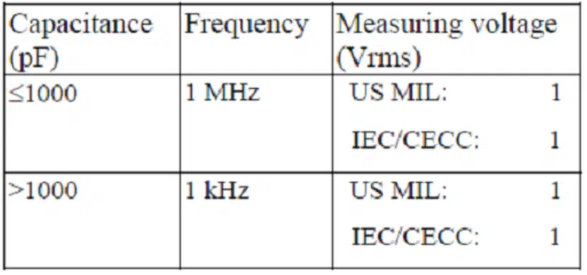
At IR and voltage strength tests sometimes in MIL and IEC/CECC a charge and discharge limitation of maximum 50 mA is specified. Comments: These limitations probably are based on older manufacturing technologies. Some manufacturers nowadays have chosen to delete these requirements in their catalogue sheets. Corresponding voltage rise times will for capacitances above 1 nF be unrealistically low. Such capacitors manage according to performed tests as a rule at least 100 to 1000 times higher inrush currents, even at repetition frequencies in the kHz range.
Diagrams
As usual we shall present a number of diagrams describing the different characteristics versus temperature and frequency.
Temperature dependencies
Capacitance and Tan δ versus temperature
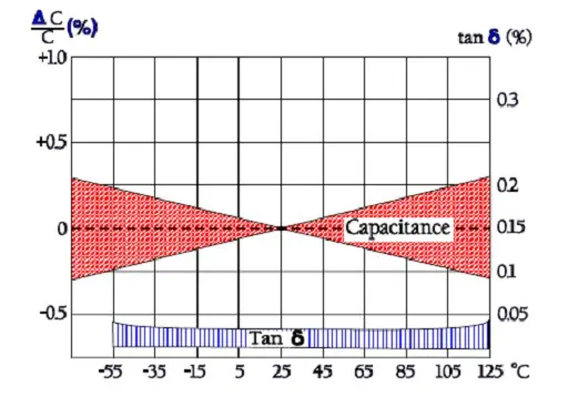
IR versus temperature
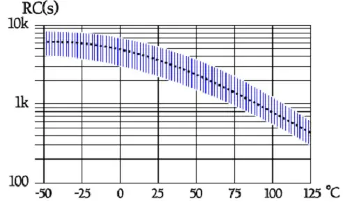
Comments to Figure 23 about RC product and IR.
When we convert the RC product to insulation resistance (IR) expressed in MΩ and go down in capacitance the IR increases correspondingly. Specifications usually set limits to the IR increase at 10 nF. Ac-cording to the typical curve in the figure RC is approximately 4000 s at 25°C which gives an IR = 4000/10(nF) = 400 GΩ. Larger values can not be expected for capacitances lower than 10 nF.
Frequency dependencies
Capacitance and Tan δ versus frequency
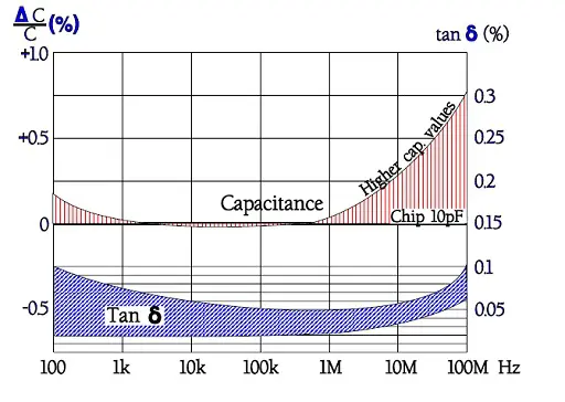
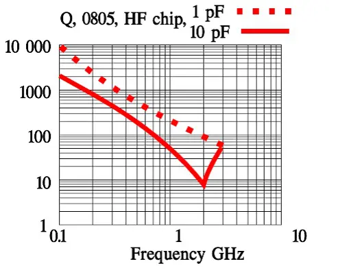
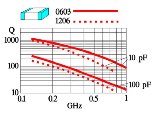
Q versus frequency
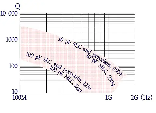
Notice how the Q value increases with decreasing capacitance and chip size. The figures 25. and 27. show examples of the same phenomenon.
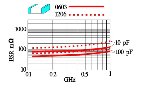
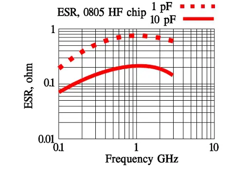
ESR for the same chip as in Figure 27. is shown in Figure 28. Other examples of the frequency dependence of ESR are found in Figures 29 to 31.
ESR versus frequency
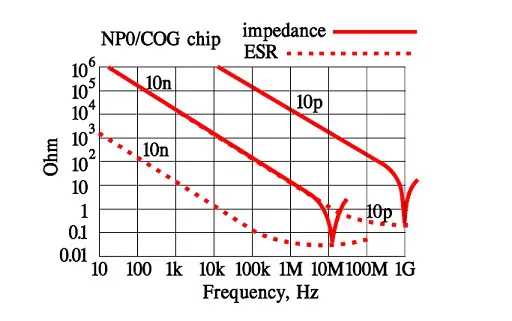
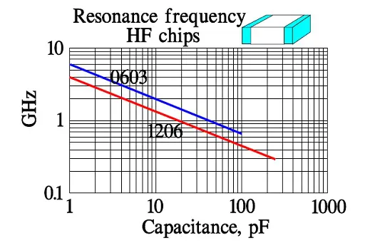
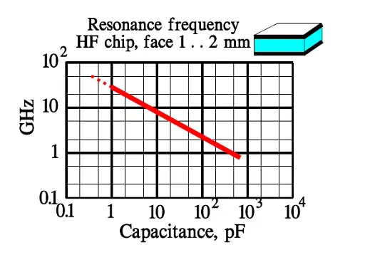
Resonance frequency versus capacitance
Examples of series resonance frequency versus capacitance for two sizes of HF chips in MLC design are shown below.
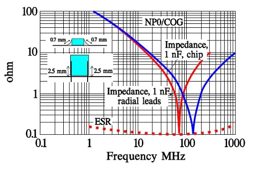
As a comparison to the MLC example above Figure 33. shows how a SLC chip in approximately the same size as 0603 may behave.
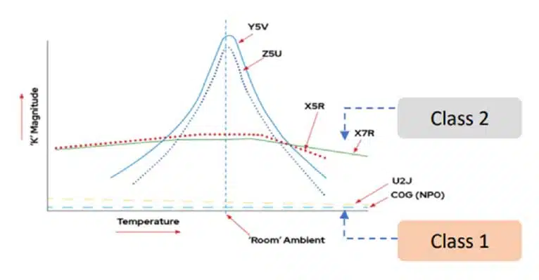
Class 2. Ceramic Capacitors
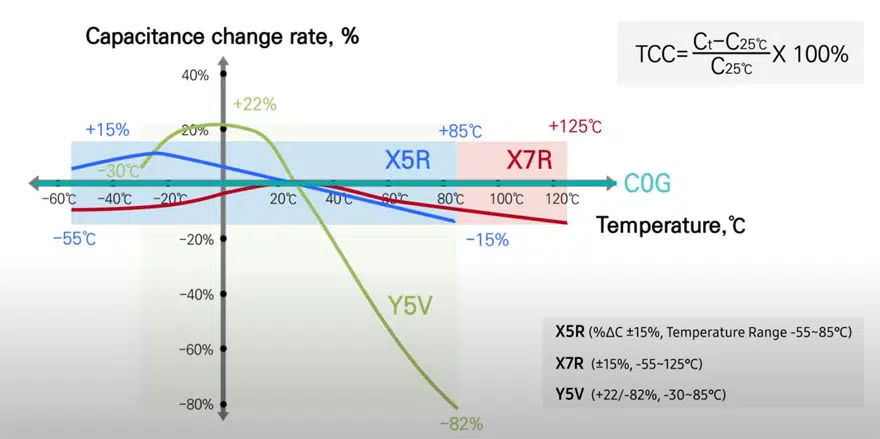
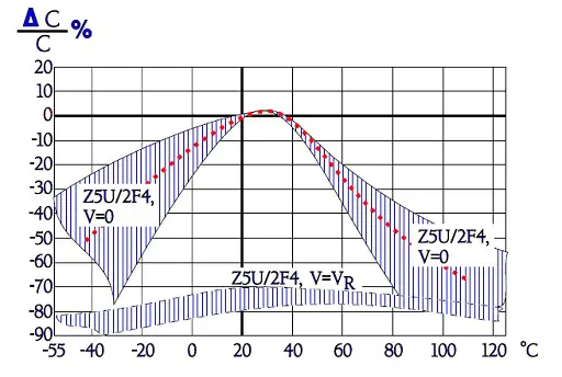
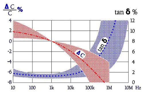
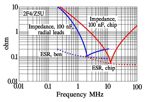
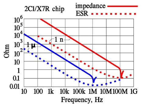
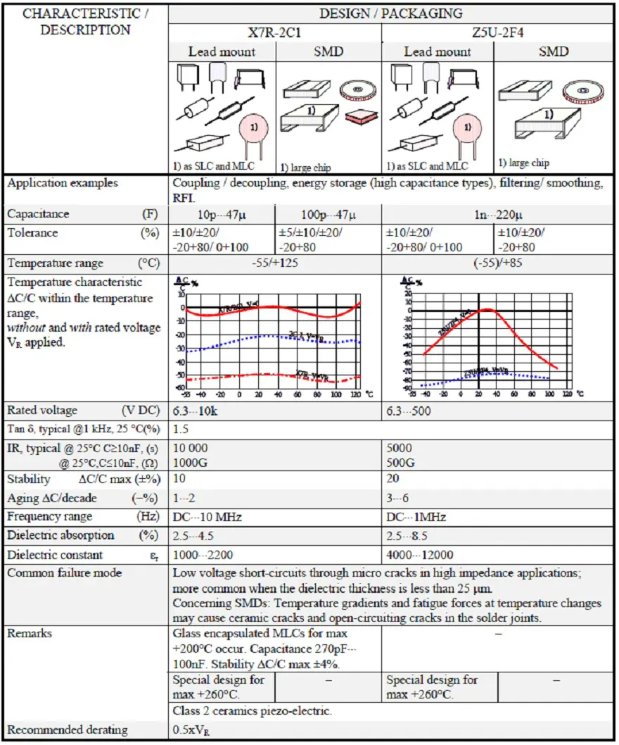
Ceramic Class 2 capacitors can be divided in two main groups, one with a moderate temperature dependence for the class – ΔC ≤ ±15% within the temperature range – and the other with such changes that only a fraction of the capacitance remains at the temperature limits. The first group is in our tables and diagrams represented by the ceramic type denominated X7R or 2C1, the latter by Z5U or 2F4.
Introduction to Class 2
Class 2 capacitors are characterized by high dielectric constants, often designated with a K followed by the εr. Hence K2000 means εr ≈ 2000. The temperature dependence of the capacitance is large. Therefore EIA characterizes the ceramic with three characters that in order state the lower and the upper limit of the temperature range and last the capacitance change within the range.
| Letter code low temperature | Number code upper temperature | Letter code change of capacitance over the temperature range |
| X = −55 °C (−67 °F) | 4 = +65 °C (+149 °F) | P = ±10% |
| Y = −30 °C (−22 °F) | 5 = +85 °C (+185 °F) | R = ±15% |
| Z = +10 °C (+50 °F) | 6 = +105 °C (+221 °F) | S = ±22% |
| 7 = +125 °C (+257 °F) | T = +22/−33% | |
| 8 = +150 °C (+302 °F) | U = +22/−56% | |
| 9 = +200 °C (+392 °F) | V = +22/−82% |
Example: X7R means with EIA designations the temperature range -55/+125 °C where the capacitance change maximum ±15%, provided the DC voltage is zero. The EIA code don’t take into consideration that the Class 2 ceramic react with capacitance reduction to DC voltages.
On the other hand certain other standards do. Here some examples.
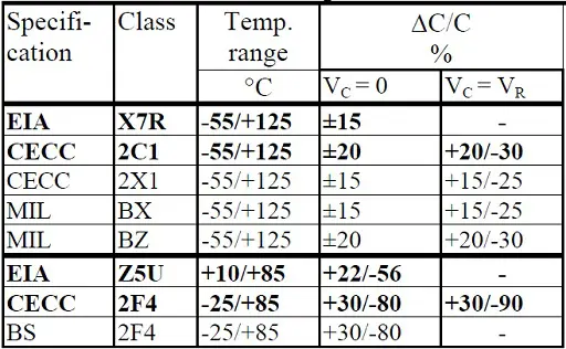
Table 5. contains two main groups of Class 2 ceramics:
• K900⋅⋅⋅K2200; ΔC approximately ±20% within the temperature range.
• K4000⋅⋅⋅K12 000; very large ΔCs at the temperature limits.
There are within these groups many more materials, for example the recent material Y5V, but in our diagrams and table information we mostly will confine ourselves to X7R/2C1 and Z5U/2F4. By specification Z5U is situated within a more limited temperature range than 2F4 but this has to do only with the specified ΔC, not with its capability to stand up to lower temperatures.
If we can accept the capacitance changes caused by cold the ceramic will stand -55°C. In the diagram section we shall look closer at the temperature dependence of the capacitance. The upper temperature limit, however, should not be exceeded. The capacitance tolerances for X7R usually are ±5, ±10 or ±20%. Usual Z5U tolerances are ±10, ±20 or -20/+80%. See also figure below.
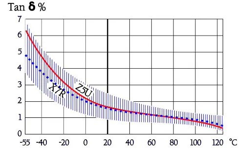
The dielectric absorption is high:
• X7R/2C1 ≈ 2.5⋅⋅⋅4.5%;
• Z5U/2F4 ≈ 4.5⋅⋅⋅8.5%.
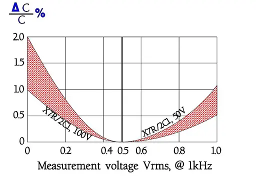
Measurement conditions
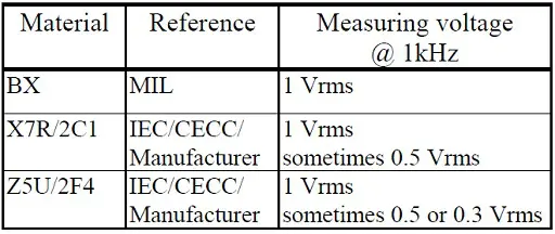
That the measuring voltage is specified and limited depends among other things on the capacitance which changes with applied alternating voltage. See examples in Figures 34 tp 38.

The Curie temperature
Ceramic capacitors have a crystalline structure and dipoles that give the materials their unique dielectric constants εr. But above a certain brittle transition temperature, the so called Curie temperature, the ceramic loses its dielectric properties. The Curie temperature for Class 2 ceramics usually is situated between 125⋅⋅⋅150 °C. The influences don’t occur at any exact switch temperature but make themselves gradually discernible in the vicinity of the Curie temperature. Thus we should rather talk of the Curie range.
C 2.11.4 The dependence of capacitance on applied voltage
Dielectric absorption (DA) and Ferroelectricity
The different types of Class 2 ceramics are based on barium titanates. Their crystalline structure are constituted by dipoles that at the polarizing present a dielectric hysteresis. With pattern from the hysteresis curve of magnetic materials they are called ferroelectric.
Figure 36. shows the capacitor charges versus applied voltage.
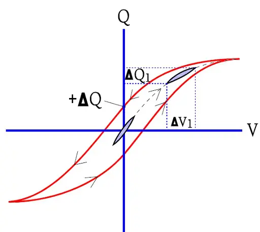
When the voltage increases from zero to a limit value and then decreases, the charging curve follows another branch that at the voltage V = 0 leaves a residual charge + ΔQ. An alternating voltage of the same magnitude will force the charging curve along the outlines of the large hysteresis loop in the figure.
If the alternating voltage is small and the DC voltage = 0, the hysteresis loop will follow the small oval in the center of the figure. Small voltage changes correspond to large charge changes, i.e. to a high capacitance. But if we superimpose a small alternating voltage on a considerable DC voltage we see how ΔV1 corresponds to fainter charge changes ΔQ1. The capacitance has dropped.
Figure 36. shows how the ferroelectric material locks a residual charge ΔQ on the electrode surface when the voltage over the capacitor recedes to zero (outer circuit short-circuited). In other words it’s a question of dielectric absorption (DA). But there is a difference, too.
The ferroelectric curve swings to the V axis while the general DA curve looks like a magnified picture of the center oval. In both cases the bound residual charge ΔQ is time dependent. If the outer circuit is short-circuited (V = 0) successively charges on the electrode surfaces are set free while ΔQ decreases.
The ferroelectric energy absorption is polarity dependent. Thus a complete re-polarizing will require more energy than the initial polarizing. But in, for example, D/A converters the pulse time may not be sufficient for a satisfactory re-polarizing.
The considerable dielectric absorption that exists in Class 2 ceramics makes them directly inappropriate for precision integrators like D/A converters, especially if there are positive and negative pulses. The crystalline structure of ferroelectric materials are maintained up to the Curie temperature.
Specific group of materials are anti-ferroelectric dielectrics as we discussed in introduction and Figure 3.
Piezo-electricity
If we expose a Class 2 ceramic material to an electric field strength it will cause faint movements in the ceramic. Inversely a mechanical pressure will create electric charges in the capacitor. The phenomenon is called piezoelectricity. BX ceramics (K900⋅⋅⋅⋅⋅⋅⋅⋅⋅K1800) exposed to chock/vibration produced in an experiment output voltages up to 40 mV3.
If we connect an X7R capacitor to an oscilloscope and bang a hammer on the component we sometimes get high voltage spikes, sometimes not. It depends not only on the way the blow hits but varies from one sample to another. The output voltage is both manufacture and batch dependent.
DC voltage dependence
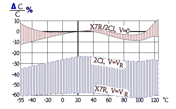
We showed just with reasoning around the ferroelectric curve how the capacitance decreased with an increasing DC voltage. How the DC voltage influences the capacitance is shown in Figure 37. Notice how specification requirements of voltage dependence affect in other respects equivalent materials.
For X7R no requirements are called for – the dependence will be great – , for 2C1 the dependence is maximized to –30%. Within the material classes the voltage dependence increases with the rated voltage. The thickness of the dielectric namely don’t grow in the proportion as the rated voltage. Thus the electric field strength increases with increasing rated voltages which in turn leads to a somewhat enhanced voltage dependence.

AC voltage dependence
Alternating voltages create a reverse effect than DC voltages on the capacitance.
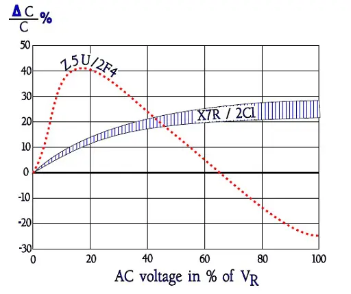
Let us emphasize that Figure 38. represent one example. Great variations may occur. In any case the significance of norms for measurements of capacitance is obvious. At IR measurements and voltage tests MIL and IEC/CECC specify a charge and discharge limitation of maximum 50 mA.
Commentary: The limitations are questionable. Some manufacturers have chosen to delete these requirements in their catalog sheets. Some even specifies voltage rise times of 1000V/μs which for capacitances above 1 nF means surge currents ≥ 1A!
If your application requires considerable charge/discharge currents, please check with the manufacturer – or test for yourself – what the capacitor can stand and restrict the application to single pulses. Class 2 ceramics don’t stand intense periodic pulse load.
Aging
Class 2 ceramics lose capacitance with time. The decrease is called aging. It is conformable to a logarithmic law and decreases with a certain per cent per time decade.
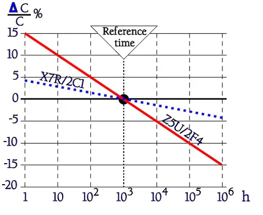
In the diagram the capacitance of the Z5U ceramic decreases with approximately 6% per time decade and of the X7R ceramic with approximately 1.3%.
Typical aging constants usually are
• BX/X7R/2C1 1⋅⋅⋅2%
• Z5U/2F4 3⋅⋅⋅6%.
The aging constant k, expressed in per cent per time decade, follows the general formula.
The capacitance decrease is defined with start 1 hour after cooling. In order to avoid disputes about delivered values relevant norms state that the value shall be guaranteed at the 1000 hrs point. With starting-point from the formula C2-2 the 1000 hrs value then is calculated as
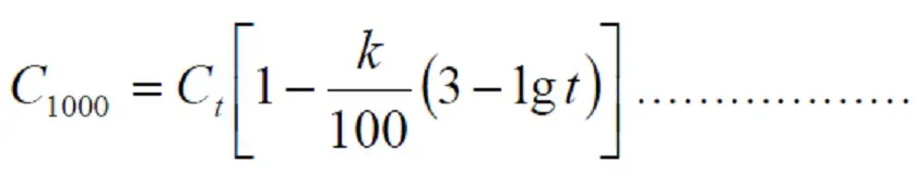
[1]
If a temporary DC voltage in the magnitude of VR is applied there will be a lingering effect in the form of a capacitance decrease more or less as if the component had been aged for 1⋅⋅⋅1½ time decade (Figure 40.).
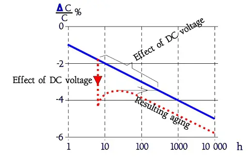
In the figure we also see how the capacitance value increases to some extent when the DC voltage – here approximately VR – is removed.
The increase can amount to approximately
• +2.5% for C21 ceramics
• +5% for X7R and Z5U ceramics.
The aging starts by definition 1 hour after cooling. Now if we heat a capacitor above the Curie point and let it cool, the crystal structures orientate themselves in the same way as after the manufacture and the capacitance resume its initial value before it, again, starts subsiding in accordance with the aging curve. One talks of “de-aging”.
Mind that every soldering of chip ceramics result in a deaging. De-aging effects may be evoked already in the lower part of the Curie range if the distance to the Curie point is compensated by a corresponding increase in time.
DC BIAS Ageing Efect
Ceramic class II capacitance loss with DC, AC, Temperature and life-time might be multiplicated and attention has to be paid to evaluate all operation conditions of final electronic hardware to make sure the capacitor meet all requirements. This is important especially in mission critical and safety applications.
An example of how much capacitance deteriorate with ageing, temperature and BIAS see the Figure below.
Read more – related articles
In-depth article presented at PCNS Passive Components Networking Symposium can be found here:
High CV MLCC DC BIAS and AGEING Capacitance Loss Explained
End users from automotive has addressed this in following articles:
Class-II MLCC DC-Bias Aging Issues in Automotive Applications
Class II MLCCs – More Detailed Classification or More Specific Default Parameters?
Capacitances of Nonlinear MLCCs: What Datasheets Don’t Tell You
Temperature dependence
Capacitance versus temperature and voltage
Tan δ versus temperature
IR versus temperature
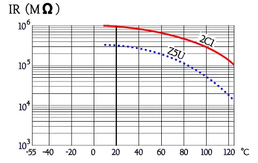
The insulation resistance in Class 2 ceramic capacitors decreases with on average one power from room temperature to +125°C typically.
Frequency dependencies
Capacitance and Tan δ versus frequency
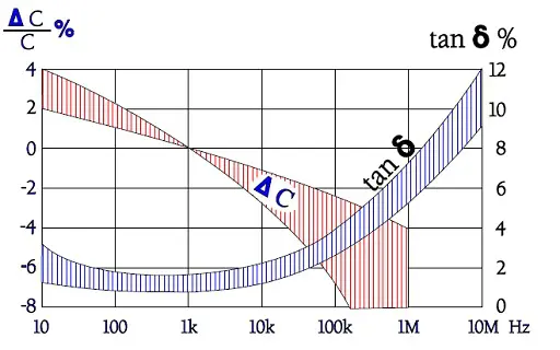
Impedance and ESR versus frequency

Frequently Asked Questions about MLCC and Ceramic Capacitors
SLCC (Single Layer Ceramic Capacitors) use a single dielectric layer, are low-cost, and suitable for RF/microwave and high-voltage applications. MLCC (Multilayer Ceramic Capacitors) stack hundreds of thin ceramic layers, offering high capacitance density, low ESR, and miniaturization, making them dominant in smartphones, automotive, and general electronics.
Class 1 dielectrics (e.g., NP0/COG) provide high stability, low losses, and linear capacitance over temperature, ideal for resonant circuits. Class 2 dielectrics (e.g., X7R, Z5U) offer higher capacitance density but with greater variation due to temperature, voltage, and aging effects, making them suitable for bypassing, decoupling, and smoothing applications.
Common MLCC failures include micro-cracks leading to short circuits, delamination during manufacturing, silver leaching in soldering, and capacitance loss due to DC bias, temperature, and aging. Flexible terminations and high-reliability grades are used to mitigate these risks in automotive, industrial and aerospace applications.
MLCCs enable extreme miniaturization, high-frequency performance, and cost-effective mass production. They are essential in smartphones, automotive electronics, power supplies, and RF circuits, making them the most widely used capacitor technology today.
How to Select the Right Ceramic Capacitor
- Define Application Requirements
Identify whether the capacitor is for resonant circuits, decoupling, filtering, or high-voltage use. This determines whether Class 1 or Class 2 dielectrics are appropriate.
- Choose the Dielectric Class
Select Class 1 (NP0/COG) for stability and low losses, or Class 2 (X7R, Z5U) for higher capacitance density with acceptable tolerance variations.
- Select Case Size and Capacitance
Follow EIA or IEC standards for case sizes (e.g., 0805, 0603, 0201). Balance capacitance value with physical size and reliability requirements.
- Consider Voltage and Reliability
Ensure rated voltage exceeds operating voltage. For automotive, industrial or aerospace, use high-reliability MLCCs with flexible terminations to prevent cracking.
- Verify Manufacturer Specifications
Check datasheets or manufacturers simulation tools for ESR, ESL, capacitance tolerance, and aging behavior. Select trusted manufacturers with proven quality control.