
source: EDN article
Don LaFontaine -March 15, 2017. With more than 500 conventional sensors monitoring the condition and performance of various subsystems on a medium sized spacecraft, there is a growing need for precision radiation tolerant instrumentation amplifiers, also known as INAs or in-amps. Many of these sensor applications use in-amps to condition small signals in the presence of large common-mode voltages and to convert a signal from one ground or offset environment to the ground or offset environment of the load. This functionality is the main reason in-amps are chosen for sensor applications where a plethora of sensors report telemetry test points and various mission-critical system statuses.
This article introduces a new architecture for radiation tolerant in-amps that overcomes some of the common drawbacks of the traditional in-amp. We’ll discuss the generic three op amp in-amp and symmetrical GM current-feedback in-amp, including their drawbacks. We’ll then examine the architecture design philosophy and benefits of two radiation tolerant, differential-ended and single-ended in-amps.
Three op amp in-ampFigure 1 shows the block diagram of a three-op amp in-amp. The high input impedance is achieved by using the non-inverting inputs of the input stage, without having to resort to any feedback tricks. The three op amp circuit strips off the common-mode voltage and amplifies the sensor signal with very little error.


Figure 1: Three op amp in-amp and its voltage nodes
The op amp action of A1 and A2 applies the differential voltage across the gain-setting resistor RG, as shown in Equation 1.

Drawbacks of the three-op amp in-amp architecture:
- The matching of the four R resistors sets the common-mode rejection ratio (CMRR), and it is difficult to obtain better than 80dB values at low gain.
- The lowest gain is one. The circuit does not offer attenuation, which is increasingly required by modern low-voltage ADCs to interface to traditional ±10V signal ranges.
- External gain resistor’s (Rext) absolute value will not match the internal R-values. The tolerance between on-chip precision resistor values and external resistor values can be 20% and as high as 30%.
- Rext tempco will not track that of the internal resistors. The tempco of integrated resistors is generally no better than 50ppm/C.
- Parasitic capacitance at each Rext pin will cause gain peaking of the input and feedback amplifiers.
- External op amp is required to drive VREF because the current through VREF varies with signals and common-mode voltages. If R=10k, then maintaining 80dB of CMRR requires the impedance of whatever drives VREF to be no more than 0.1 Ohms.
Symmetrical GM current-feedback in-amp
A more economical topology is the symmetrical-GM current-feedback implementation shown in Figure 2.

Figure 2: Symmetrical GM current-feedback
When an input signal unbalances the input GM, the output of the summation is not zero. The high gain at A creates an output voltage Vo, which through feedback unbalances the feedback GM to cancel the input GM imbalance. This way, the nonlinearities and gain variations of the simple GM stage are cancelled by equal and opposite errors of the two GMs. Note that there is no coupling of input dynamic range and feedback, or output dynamic range. The symmetrical GM current-feedback in-amp design allows for very flexible applications.
The drawbacks of this architecture are:
- Its ultimate accuracy is not more than 0.1% and it cannot deal with ±10V instrumentation signals.
- Offsets are hundreds of microvolts to 1mV.
- The finite gain-bandwidth product of the input amplifiers causes an overall -3dB bandwidth reduction for even modest gains.
A new in-amp design philosophy for space flightThe ISL70617SEH and ISL70517SEH are high performance, differential and single-ended output instrumentation amplifiers, respectively. They are designed for precision ADC applications, and both parts are tested to total ionizing dose of 75krad(Si) at +25°C with exposure at a low dose rate of <10mrad(Si)/s.
New in-amps offer several benefits:
- Allow a wide range of gains, including attenuation
- Support gain error down to 10ppm
- Remove the on-chip component tolerances from the overall gain accuracy with external RF/RIN
- Completely de-couple input from feedback effects
- Provide CMRR>100dB at gain=1
- Limit the output swing to never excessively overdrive a load by powering the rail-to-rail output stage on the load’s own power supplies, which are independent of the in-amp’s input stage supplies
- Provide input offsets of <100uV and input noise <10nV/rt-Hz and input bias currents <2nA
- Use a current-feed architecture to provide a -3dB bandwidth that does not roll off directly proportional to gain
- Enable optimization of output noise and offset for the required output swing
This is a tall order, and no simple circuit accomplishes it. The topology of the single-ended output ISL70517SEH is shown in Figure 3 and the topology of the differential output ISL70617SEH is shown in Figure 4.


Figure 4: ISL70617SEH differential output instrumentation amplifier topology
The design of both amplifiers is an elaboration of the simpler current-feedback approach. As such, bandwidth is determined by the value of the RF resistor. The highest bandwidth will be available at the lowest RF. For stable operation, the minimum RF value is 25kΩ. The GMs are implemented with two external resistors and very high-gain amplifiers that impose input and feedback voltages upon them. The feedback network is a wire from VOUT to the feedback pins. The amplifiers have gains around ten million and linearize the transistors errors well below the 10ppm level. With very high gain in the pseudo-GMs, the circuit adds little gain error and only RFB and RIN set gain to the 10ppm level. Resistor cost can be tailored to the accuracy needed. Note that the input stage is completely unaffected by output biasing, which is ideal for an instrumentation amplifier.
The VREF pin on the ISL70517SEH and the VCOM pin on the ISL70617SEH are inputs to a very low bias current terminal, and require no external buffer amplifier. These pins would be connected to a mid-scale voltage when driving an ADC, such that the input would have a ± input signal span when driving a single-supply ADC.
The output linear dynamic range is set by ±100uA*RF as set by the class-A biasing from the 100uA internal current sources. While the output will continue to move with overloads beyond this value, it will not be linear. The output stage is a rail-to-rail design, and has separate supplies from the rest of the IC.
A typical supply arrangement when driving a 5V ADC is to have VCO connected to the ADC’s +5V supply, and VEO to ground. Thus, the ADC can never be overdriven beyond it supply rails. This also reduces power dissipation when the main supplies are set to ±15V, since about half of the total supply currents go to output supplies.
Similar to the resistor-oriented op amp topology, parasitic capacitance at the RF node will peak the frequency response. The ISL70517SEH and ISL70617SEH are tolerant to parasitic capacitances at RF from values of 2pF to 20pF. The input stage is even more tolerant, allowing 2pF to 30pF. The RF and RIN resistors are provided with Kelvin sense pins to minimize interconnect resistance errors. This is especially useful at high gains and small RIN.
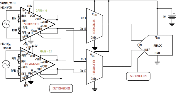
Space-grade analog signal chain application examples
Figures 5 and 6 show a complete space-grade analog signal chain for both in-amps. These examples show the in-amps in a gain of 10 and a gain of 0.1. Their outputs are then multiplexed with the radiation tolerant ISL71830SEH 5V 16-channel multiplexer into a radiation tolerant ADC. Notice the output stage of the in-amps and multiplexer are both powered from the ADC supply. This feature enables the output to be driven by the same low voltage supplies powering the ADC, thereby providing protection from high voltage signals and the low voltage digital circuits.

Figure 5: ISL70517SEH single-ended output space-grade analog signal chain

Figure 6: ISL70617SEH differential output space-grade analog signal chain
Conclusion
A radiation tolerant instrumentation amplifier is ideal for high performance sensor signal processing applications in space. The new design architecture presented in this white paper has several advantages over the typical three op amp in-amp design and the symmetrical GM current-feedback in-amps.
The new differential and single-ended output in-amp architecture enables high levels of DC precision and excellent AC performance, and has features not found in other in-amps. The ISL70517SEH and ISL70617SEH feature a wide range of gain (including attenuation), gain error down to 10ppm, typical CMRR 120dB @ gain equal to 1 and a rail-to-rail output stage that can be powered from the same supplies as the ADC, which preserves the ADC maximum input dynamic range and eliminates ADC input overdrive.
Their precision and rad tolerant performance makes these amplifiers ideal in analog sensor front ends, shunt current sensing, and instrumentation and data acquisition applications that require very low noise and high dynamic range in the space environment.
About the author
Don LaFontaine is a senior principal applications engineer with Intersil Corporation’s Precision product line, and is located in Palm Bay, Florida. His primary engineering focus is on precision analog products. He received his BSEE from the University of South Florida.

