
source: Power Electronics news
Apr 10, 2017 Slobodan Ćuk, TESLAco, and Sam Davis, Power Electronics. Virtually all present-day DC-DC converters store DC energy in magnetic devices with ferrite cores, such as inductors with DC bias. A new topology for non-isolated step-down dc-dc converters discards ferrite cores completely. The new Resonance Scaling Method results in use of 10nH resonant inductors even at 50kHz switching frequency and an effective factor of 1,000 times reduction of the magnetic size and weight of comparable buck converter at 50kHz.This opens a new power electronics era with the first true Power-Supply-on-a-Chip.
The groundbreaking PWM-Resonant Ćuk topology could revolutionize the design of non-isolated, step-down dc-dc converters. This new topology provides much higher-efficiency, fast-transient response settling in one cycle, with much smaller size and lower weight than its ferrite core cousins. This converter is ideal for 12V to 1V applications for supplying microprocessors, as it replaces four to eight modules of a multiphase buck converter with a single converter.
Obviously, it is equally beneficial in all step-down voltage applications. This topology reduces 10 nH resonant inductors to copper traces on the board at even 50kHz and enables high-power, ultra-high efficiency, and unprecedented power density at reduced cost.


Buck Converter Fundamental Flaw
Invention in 1831 of AC transformer by Michael Faraday and AC inductor by Joseph Henry introduced for the first-time alternating components AC inductors and AC capacitors into Electrical Engineering which until that time only knew for resistors and Ohms law. Modern Power Electronics was founded in 1950’s based on the buck converter which used inductor for reducing output ripple current. That inductor needed to pass the full DC load current.
Yet, AC inductor could not pass even a minute mA currents without saturating magnetic core and making it effectively a short circuit instead of a large inductance. The solution was found in “inventing” a new magnetic component, termed here a “DC inductor” by inserting an air-gap in series with the magnetic. This forever condemned buck converter and its many derivatives to limited DC load current and limited power. Unfortunately, IEEE standards committee never got around to define a new symbol for such an altered component with very limited power capabilities.
Air-gap increase and inductance decrease
Increase of DC load current results in increase of DC ampere-turns NIDC (product of number of turns N and DC load current IDC). This, in turn, requires the proportional increase of the inserted air-gap and a very rapid “killing” of inductance value. This is illustrated by the “moving viewgraph” and the related flux-linkage vs IDC characteristic display in the below video clip.

New Switching Method and Topology with Two Resonant Inductors
Obviously, there was all along a need to eliminate this DC inductor of buck converter and replace it with one or more resonant inductors which would in a single stroke eliminate both DC current and power limitations of the buck converter. To achieve this required several complementary groundbreaking inventions:
- New switching method with two resonant inductors, defining two switching subintervals, each consisting of separately controlled resonances.
- Appropriate switching devices topology limiting each resonant current to only its positive current to establish voltage regulation using conventional duty ratio control and constant switching frequency.
- Resonances Scaling Method to reduce inductances to ultra-low values even at moderate to low switching frequencies of 50kHz or less.
This is accomplished in the PWM-Resonant Ćuk converter shown in Fig. 1. This converter features two complementary active switches operating out of phase with each other and at constant switching frequency and variable duty ratio, D, of the main switch, S1. Two passive switches, diodes CR1 and CR2, operate in synchronism with related active switches to form two effective voltage bidirectional switches. Turning on switch S1 turns ON diode CR1. Likewise, turning ON switch S2 turns ON diode CR2.
This new converter topology uses two air-core ac inductors that do not need coil windings. Based on new and general Resonance Scaling Method, the two inductances can be as low as 10nH, even at low 50kHz switching frequency. The resonant inductors can be implemented with only 5mm long or shorter copper wire or as a short trace on a circuit board.

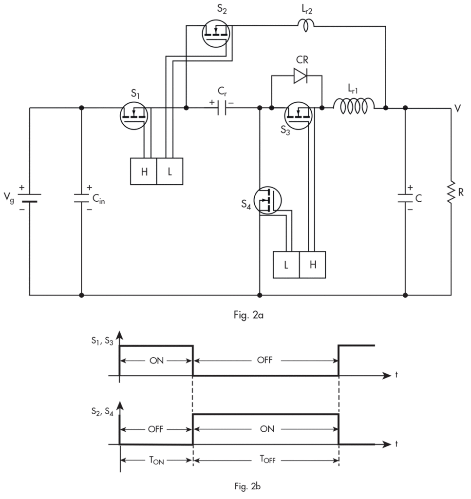
For low-voltage applications, you can replace the two rectifier diodes with synchronous rectifier MOSFETs (Fig.2a), which reduces conduction losses. This circuit with two high-side drivers is shown in (Fig. 2b). These high-side drivers are practically implemented in the 200W prototype (Fig.4) with two MOSFETs on the left working as S1 and S2 switches, and two MOSFETs on the right operating as synchronous rectifier MOSFETs. Note also that switch S3 shows a diode CR highlighted across the MOSFET transistor. This signifies that this MOSFET must be controlled to emulate the switching operation of that diode and not allow the current flow in opposite direction. This will keep the resonant current ir1 always positive so that each cycle it starts at zero current level and stops at zero current level as seen in second trace of Fig. 4.
Note also that due to current-bidirectional nature of MOSFET switches, this implementation is also bi-directional in current and power flow.

Also, you can replace all four MOSFETs with GaN transistors as shown in Fig. 3. GaN transitors have about four times smaller footprint than the equivalent transistors based on silicon. Thus, four GaN devices could be integrated onto a single IC chip in a package usually used for a single low-voltage, high-current MOSFET. GaN transistors have also an order of magnitude lower parasitic capacitances. Moreover, when these GaN switches operate at 50kHz, instead of their typical 2MHz used for buck converters, they allow hard switching with negligible losses and high efficiency at these much reduced switching frequencies.
Topology with Two Resonant Inductors
This converter (Fig. 1) has three resonant components: resonant capacitor Cr, resonant inductor Lr1, and resonant inductor Lr2. They, in turn, create two overlapping resonances (Fig. 4):
- First resonance between resonant capacitor Cr and resonant inductor Lr1 (second trace)
- Second resonance between resonant capacitor Cr and resonant inductor Lr2 (third trace)

Note that full sinusoidal resonance is prevented and only positive cycle of each resonance is permitted due to current unidirectional feature of each diode rectifier. Hence, each resonance starts at zero current level and stops at zero current level as seen in the second and third trace of Fig. 4. This is the reason for the ultra-fast transient response obtained in the experimental verification of Fig. 5, where any dc load current transient is settled in one switching period.
In fact, the dc load current Idc dictates the magnitude Im of each respective resonant current. The dc load current then dictates both magnitudes of the two resonant peak currents, which are by nature, always starting and ending at zero current level such as seen in Fig. 4. It is not surprising then that the experimental measurements in Fig. 5 show that the large step-load current transient is settled in a single switching period and using only one converter module. Typical multi-phase buck converter demands at least four and often up to eight converters operating in parallel, and even then requires at least 10 to 20 switching cycles to settle the tranients with acceptable voltage overshoot. This, in turns, dictates 1MHz or higher switching frequency in order to satisfy fast transient requirements of microprocessor power supplies. This is obviously due to an inherent dc energy storage in an air-gap of each constituent buck converter module.

Measurement of the voltage conversion ratio as a function of the duty ratio, D is seen in Fig. 6. Note that the converter has intrinsically a 2:1 voltage step-down. In this example, the further voltage step-down is obtained for duty ratios below D = 2/3. At which point that happens is a design choice. Note also that for low duty ratio the step-down voltage conversion follows linearly the operating duty ratio, like in a buck converter. The input current waveform and output current waveforms are displayed in Fig. 7. Note that each of the two ac resonant inductors contribute their respective currents to the load, making the load current waveform trapezoidal in nature. The direct benefit is that the ac ripple current is much reduced below dc current load and therefore the size of the output capacitance significantly reduced when compared to the buck converter. This leads to dc conversion ratio being controlled by reduced input current pulse due to reduced duty ratio D as in Fig. 7. Consequently, an opposite large dc voltage reduction ratio is obtained at low-duty ratios as illustrated in measured dc voltage ratio in Fig. 6.
Ultra-High Efficiency
An early experimental prototype of a 200W, 48V to 24V, step-down converter was built (Fig. 8). Efficiency measurements shown in Fig. 9 demonstrate ultra-high efficiency over 99% over wide current range from 3A to 12A and nearly 99% at the full load of 15A. As shown in Reference (UP Patent No. US 8,134,351), the equivalent buck converter inductor would need the ferrite core (Fig. 10) with core cross-section of 240mm2 and 5 turns. In a PWM-Resonant Ćuk converter an effective 40 times reduction of ac flux is achieved. This permits only one-turn inductor on a ferrite core with only 30mm2 core cross section. This magnetic realization is shown with ferrite core in the middle of the prototype in Fig.8. This earlier prototype did not use the best available chip capacitors presently available.

A much-reduced output filter capacitor is sufficient to obtain a low output ripple voltage. Finally, note the overlapping conduction of two resonant currents. This interval is characterized with the liner reduction of the resonant inductor current ir1 and the discharge of resonant inductor Lr1 into the output.
Series Resonant Circuit Analysis
To simplify analysis of the resonant circuit assume that two resonant inductances are identical so that Lr1 = Lr2 = Lr , leading to a single resonant frequency fr. Also assume that the switching frequency fs is also close to this resonant frequency but lower than the resonant frequency. This does not affect the generality of the analysis below. In fact, using ultimately different values for two resonant inductances leads to the further optimization of the practical designs. Likewise, choosing the switching frequency appropriately leads to additional design optimization.
The resonant equations and solutions are:

Where:
RN = Characteristic resistance
ωr = Radial frequency
fr = Resonant frequency
Δvr = Resonant capacitor ripple voltage
Idc = Average dc load current
Im = Peak current
Resonance Scaling Method
The conventional PWM control of buck converter has only one way to reduce the value of the buck inductance, hence the size and weight of inductor. This is done by proportionally increasing the switching frequency to 50 MHz in order to keep ripple currents from growing without bound with reduced inductance value. This is not the case with the PWM-Resonant Method, which, as demonstrated in prototype of Fig. 8, which has already reduced the magnetics size by a factor of 40. The implementation in prototype of Fig. 8b did not take into account that another factor of 100 and more of further reduction of resonant inductor values is made possible by the newly discovered Resonance Scaling Method of scaling down resonant inductance values by a factor of 100 or more at any switching frequency as described herein.

This Resonance Scaling Method is based on reducing the resonant inductance values while at the same time increasing proportionally resonant capacitance to keep the resonant frequency and switching frequency unchanged. Once the scaled down resonant inductances are so small, like 10Nh they can be replaced each by the short trace on the board layout even at 50kHz. In the scaling down process of resonant inductance values, the magnetic core is naturally shed at any switching frequency and the inductances freed from the “shackles” of the ferrite cores and its hazardous saturation. Furthermore, the associated core losses of the ferrite cores are also eliminated while the weight is dramatically reduced as well. The magic of the new Resonance Scaling Method brings single-handedly another factor of 100 reduction of magnetic components on top of the already discussed factor of 40 for a total reduction of 4,000 times. Thus, it should not be surprising that in order to match another 200W, 12V to 5V, 40A converter using PWM-Resonant Cuk converter at 50kHz, the PWM buck converter would have to operate at around 50MHz switching frequency. (see later section on Buck converter at 20MHz).
This new method to scale down both resonant inductances at any switching frequency is now explained in more details using simplified choice that Lr1 = Lr2 =Lr. This is possible due to two resonant component variables, resonant capacitor Cr and resonant inductor Lr. Instead of a single inductance L in PWM method, and for Im =1A we choose for starting design:
Lr0 = 1μH Cr0 = 1μF, RN0 = 1Ω Δvr =1V fr = 133kHz (9)

Note that there are literally hundreds of combinations of resonant components which will keep the same resonant frequency of 133kHz. Obviously increasing inductance and decreeing capacitance must be ruled out from efficiency and size viewpoint, as capacitive energy storage and transfer is much more effective in terms of size, cost, and efficiency. Hence, we will limit ourselves to the reduction of the resonant inductance and proportional increase of resonant capacitance with a proportionality factor (n) to get:
Lr = Lr0 /n Cr = Cr0/n RN = RN0 /n Δvr = RNIm (10)
For a hundred-fold reduction of inductance (n = 100):
Lr = 10nH Cr = 100μF RN = 0.01Ω Δvr = 0.01V (11)
The resonant peak current could now be increased hundredfold to Im= 100A corresponding to Idc = 70A dc load current as per Eq. 8 to still result in the same ripple voltage Δvr =1V for a converter with output voltage 5V and 500W power. Therefore, the same resonant frequency of 133kHz is maintained but with a much lower resonant inductance using only 10nH, and yet processing 500W power.

Scaling resonant frequency to 50kHz
An argument could be made that a 100μF chip capacitor cannot handle 100A or 1A/μF. This is not a problem: the resonant capacitor value could be increased by approximately seven times to 700μF to reduce the frequency to 50kHz and still keep resonant inductances at 10nH.
For example, 12 chip capacitors (Fig. 10) in 2012 size and each with 45μF will result in 540μF total capacitance. With each capacitor rated for 4A rms current at 50kHz, this will give a total 48A rms current capability, sufficient for 40A dc load current of the 200W example. Obviously, the higher power will naturally be handled more efficiently at lower switching frequency.

Three Myths of Power Electronics
Dr. Slobodan Ćuk of TESLAco, who invented this topology, says there are three myths of Power Electronics technology. He says the Power Electronics “dream” for decades has been to eliminate the ferrite cores by going to ever higher switching frequencies? Here is one of three big myths related to that. First myth:
Do We Need More or Have All Topologies Been Invented?
PWM-Resonant Ćuk converter demonstrates that newly invented better topologies are already here! The proper question to ask is instead: should we keep the obsolete topologies like a buck converter?
The second myth:
Do We Need GHz Switching frequencies for Very High Power?
PWM-Resonant Ćuk converter demonstrates just the opposite: the efficient usage of resonant capacitors and inductors naturally impose: reduction of inductance values while even using proportionally larger increase of resonant capacitor values, clearly is the most efficient use of both components. This clearly leads to natural reduction of switching frequency for higher power even without accounting for terrible effect higher switching frequency and higher power have on switching losses, EMI,etc. All switching devices also operate much more efficiently at lower switching frequencies.
The third myth:
Power Supply on Chip (PwrSoC) vs Discrete Designs!
Size and weight of magnetics components has always been forced in the past the Discrete Designs. PWM-Resonant Ćuk converter reduces resonant inductors to copper traces on the board at even 50kHz. This opens up a new Power Electronics era with the first true very high Power Supply on a Chip (PwrC) solution and simultaneously dramatically increased power density as well as overall efficiency.
The comparison of the inductive energy storage and transfer of buck converter and resonant capacitive storage and transfer of PWM-Resonant Ćuk converter in Fig. 10 clearly shows the winner!
Comparison with Buck Converter at 50kHz
It is now very instructive to make the comparison with a buck converter operating at 50kHz for the same 200W, 12V to 5V, 40A step-down conversion. To make it easier to follow the calculations, assume that the magnetic core used has 200mm2 core cross-section, which is close to an RM14 core in Fig. 10. To get a reasonable ac flux density, five turns should be used. Instead of actually calculating the air-gap needed to support 200 dc ampere-turns, the resultant inductance is calculated from:
L= NBdc S/ Idc = 5 x 0.1T x 200mm2 / 40A = 2.5μH (12)
N = Number of turns, which is 5, and Bdc = dc flux density 0.1 T corresponding to 40A dc load current.
Note that the inductance needed by a buck converter for the same design is 250 times higher and yet there is no point in making a size and weight comparison with two 10nH inductors implemented with 5mm copper trace of PWM-Resonant Ćuk converter. The buck converter inductor will also have additional sizeable core losses despite its five turns as well as much larger copper winding losses so that comparison of losses is also pointless, as is the cost comparison.
Buck Converter at 20MHz?
Where did the demand for 25 MHz switching for buck converter come from? The thought was that by just going to high enough switching frequency, the buck converter could finally shed its ferrite magnetic core and dc bias limitations and be used just as a coil winding without magnetic core. As the solution is already presented that employs just two small 10nH inductors, it would be instructive to see as to what switching frequency buck converter must operate to match that.
For 5V output and using 10nH inductor at 20MHz, the output ripple current of the buck converter would be 25A, as per formula:
Δi = VD / (fr Lr) = 5Vx 0.5 / (10MHz x 10nH) = 25A (13)
Simulation results for the 5V, 40A converter shows the rms ripple current in output capacitor of PWM-Resonant Ćuk converter at 50kHz to be only 10Arms. Perhaps then even 50MHz switching frequency might be needed.
One practical engineering thing must not be overlooked. Advocates of GaN buck converter design at 2 MHz are cautioning engineers that a special very careful layout design is needed at those switching frequencies with 100nsec on time of main switch for a 48V to 1V, 100A converter design. Imagine this multiplied by a factor of 10 or 25 for 20MHz and 50MHz buck converter design.
Figure of Merit for Switching Devices
Classical trade-of exist for all active switching devices (transistors) based on the Figure of Merit (FOM) defined as:
FOM = (Gate to source capacitance) x (ON resistance) (14)
Therefore, instead of 500kHz MOSFET device designed for the minimum combined total losses of gate drive and conduction losses, the new MOSFET devices could be optimized for 50kHz so that much reduced gate drive losses at 50kHz are traded for corresponding reduction of the dominant conduction losses by reducing ON resistance of the MOSFETs at modest increase of gate drive losses. Same appears to be true for design of new GaN devices SiC MOSFET devises and even IGBT devices. This would eliminate the need to reduce conduction losses by paralleling many devices with only limited success to reduce total conduction losses (current sharing problem) while simultaneously increasing gate drive switching losses.
Power Supply on the Chip (PwrC) Applications
For the very first time a true Power Supply on a Chip (PwrC) step-down dc-dc converter has been achieved. This clearly opens up many exciting applications, which either have not been previously possible or were much inferior in size, weight, efficiency and cost.
In the first category, one important application comes first to mind:
- Fast, on-board dc-dc battery chargers for fully electric vehicles (FEV). At present, fast battery chargers cannot be placed on-board due to their extreme size and weight and are available as standalone units only at very high cost. The new PWM-Resonant Ćuk PwrC technology makes possible a 25kW, 400V fast battery charger to be placed on-board at much reduced cost. The use of latest GaN transistor and SiC MOSFET transistors would further reduce the size and increase power capability of a single module.
In the second category are:
- Replacement of high power Intermediate Bus Converter, such as 1kW, 48V to 12V dc-dc converter with 99% efficiency dc-dc converter at much reduced size and cost.
- Use of a single 12V to 1V converter module for microprocessor power supplies exhibiting fast one-cycle load transient response, high 99% efficiency and ultra-compact size due to PwrC property.
- Due to 99% and higher efficiency and PwrC technology, even a two- stage approach, such as 48V to 12V converter followed by 12V to 1V converter might also be considered to replace present inefficient and bulky two-stage approaches.
Many other applications will no doubt be revealed soon.
Passive Components, Capacitors and Inductors are Mandatory for Mega Watt Power Conversion
Exclusive emphasis on Development of Switching Devices at ever increasing switching speeds has led to the claim that devices such as Silicon Carbide MOSFETs will enable Megawatt power and offset their higher cost. This is propagating the false claim that all we need is high power switches as SiC MOSFETs and completely neglecting that the Electric Power Conversion cannot be accomplished by Switching devices alone. The passive components, capacitors and inductors are needed equally to facilitate smooth and efficient energy and power transfer from input to output.
Capacitive energy transfer and switches alone are apparently not effective as confirmed by Switched Capacitor converters which are limited to several Watts of power, no regulation and very low efficiencies below 60%. Present power converters (buck, boost, flyback, etc.) are employing exclusively inductive energy transfer using DC bias inductors and switches and are now also proven not to be suitable for Mega Watt power conversion.
PWM-Resonant converter technology described here proves that in addition to high power MW switches both capacitive and inductive energy transfer are mandatory. Moreover, the energy density of MLCC capacitors is orders of magnitude higher than that of the inductors with ferrite cores. This then leads naturally to elimination of ferrite cores and reducing inductive energy transfer to low value inductances without ferrite cores as described herein.
Yet the two resonance methods introduced along with breakthrough Resonance Scaling Method enables those small 10nH resonant inductors to share and carry equal burden of large energy and power transfer as their equally compact MLLC capacitors. Moreover, for the first- time Power Supply on the Chip made possible as the Power Devices small size and efficiency are matched by equally small size and efficiency of the passive components, the energy transfer capacitors and resonant inductors.
Conclusion
Power Electronics has been for the last 60 years focused exclusively on the development of ever faster switching devices from 20kHz bipolar transistor through 200kHz MOSFET devices to present 2MHz GaN devices. In fact, it is precisely the availability of the high frequency switching devices which was, all along, hiding the fundamental flaws of the buck converter and delayed the inevitable conclusion: the buck converter should now be retired.
In engineering designs we are accustomed to hail 40% improvement in size as a milestone achievement. The PWM-Resonant Ćuk converter has already resulted in 40 times size reduction over buck converter (Fig. 8). The new Scaling Method generated another factor of 100 reduction in size of magnetic components for a total factor of 4,000 times reduction in magnetic size (Fig. 10). The simultaneous high efficiency of over 99% and ultra-small size of magnetics makes for the first time possible both Power Supply on the Chip (PwrC) with ultra-high power density and at the same time extremely compact size with minimal or no heat-sink depending on power level.
The novel PWM-Resonant Ćuk converter proves that the new switching methods along with the corresponding novel topologies and the breakthrough Resonance Scaling Method are by far the most important for size reduction, efficiency improvement, simultaneous cost reduction and ultimately the best use of switching devices, both classical MOSFET and new GaN and SiC MOSFET devices. Switching device requirements are then dictated by the new switching methods and their sister topologies and not the other way around as is the case now.
This is an exciting time in power electronics as a new era begins, opening a wealth of innovations and possibilities. Tune in for the next big thing!
References
Slobodan Ćuk, “Four-Switch Step-down Storageless Converter,” Patent No. US 8,134,351 B2, March 13, 2012.

