
Source: Electronics 360 article
By Jeff Morroni, Director of Power Management – Kilby Labs.
There is no doubt that power in all its aspects – regulating, delivering and dissipating it – is an increasingly important topic. The industry is seeing significant design emphasis on power-related issues as products are expected to do more, do it better, do it smarter and do it cooler. Looking to 2019, three broad issues stand out as areas of greatest interest: density, EMI and isolation (signal and power).
Achieving higher density: Getting more power management into less space
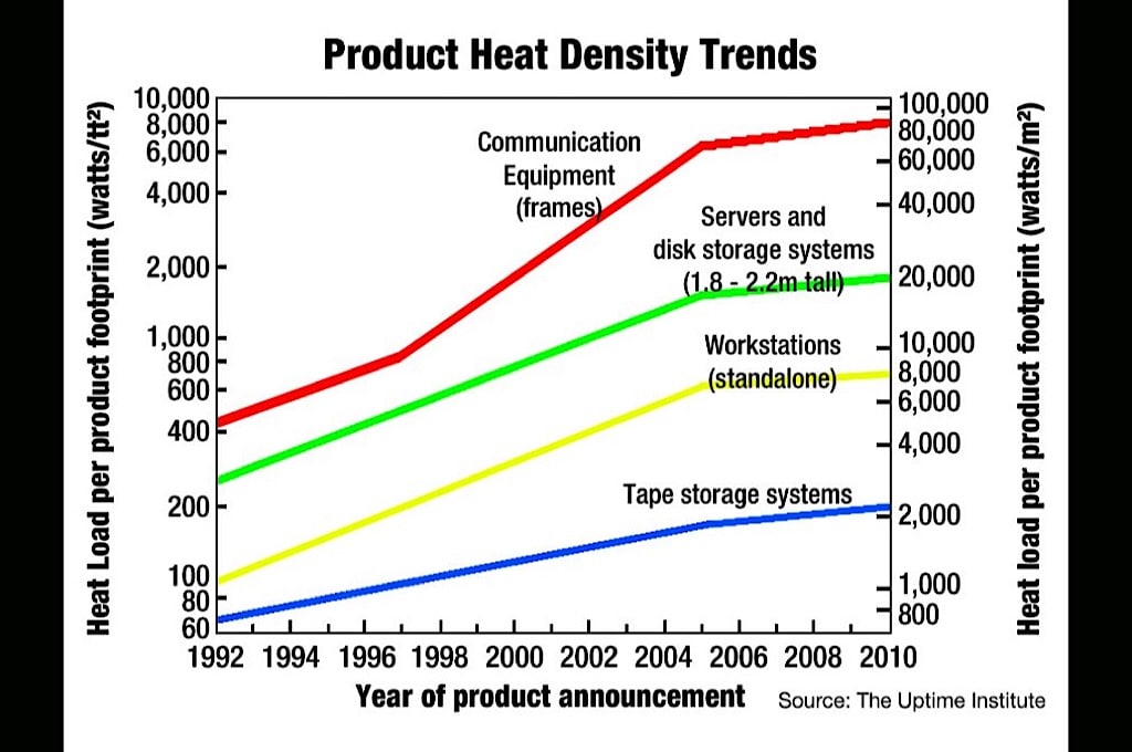
As a result of the dramatic scaling-down of IC process lithography and per-function operating power, thus allowing more functions and gates on a chip, the overall power demands on the end product have grown rapidly, featured Figure 1. Some processors now draw several hundred amps and can ramp from a low-current to fully active in less than a microsecond. It’s not a joke to say that the density goal is to “put a kW in area of a coin” via reduced losses and better thermal performance.
Featured figure 1: Product heat density trends from 1992 to 2010. Source: IEEE GlobalSpec
The problem is not just managing the power and resultant dissipation. Even apparently “negligible” resistances in the source-load path have become major impediments to effective power delivery due to basic I2R losses: at 200 A, just 1 mΩ of lead/trace resistance is a 0.2 V IR drop and 40 W dissipation. Further, using smaller converters presents a dilemma as they can be placed closer to loads, which is good for reduced trace loss and noise pickup, but also places a “hot plate” near the load, resulting in a temperature rise.
Trends related to power density: A single “magic bullet” will probably not be the solution to the density dilemma. Solutions will instead consist of interdisciplinary improvements leading to:
- higher-frequency switching;
- moving the power-management function (or its inductor) under the processor heat sink;
- higher rail voltages such as 48 V to minimize IC drop;
- new packages types;
- and integration of passives onto the die or into the package.
Reducing EMI: Emissions cause performance uncertainties and regulatory rejection
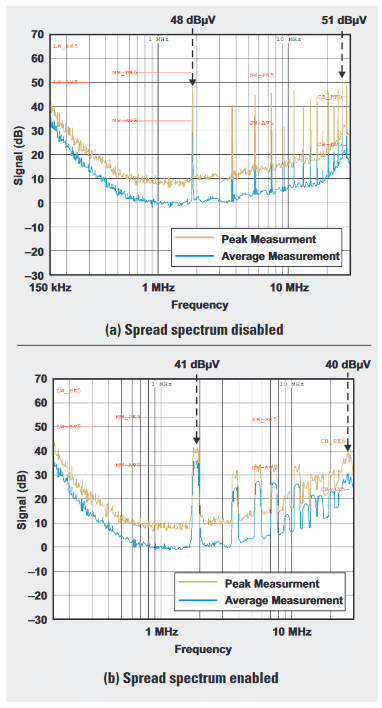

Figure 2: A noise comparison with spread spectrum disabled and enabled. Source: Texas Instruments
Reducing EMI has become a bigger issue as electronics proliferate both more widely and deeply into mass-market applications, as even a quick look at today’s automobiles proves. In fact, some EV/HEVs no longer offer an AM radio, even as an option, due to difficulty of suppressing AM-band EMI. EMI in autos has consequences beyond just the radio, of course, and can affect mission-critical ADAS (advanced driver-assistance systems) functions such as adaptive cruise-control radar.
For designers, the challenge in EMI is that it is often more an art than a science. It is a difficult problem to model and its solutions often require trial-and-error to reduce it to a desired maximum. Further, EMI is not a single entity, but has different sources, paths and appearances. For example, radiated EMI can often be a strong function of lead routing and PCB layout, while conducted differential-mode EMI is a stronger function of your converter design and passive filter network.
Trends related to EMI: Solutions such as passive filters are available and can be very helpful, but are viable only to a certain level within an acceptable penalty zone in size, weight and cost. The bigger opportunity is how IC vendors can address the EMI situation at the source, thus delivering better results and enhancing ease of use towards meeting the necessary compliance standards.
The solutions involve a detailed look at the fundamentals of noise and layering the techniques that will reduce it:
- increased use of spread-spectrum techniques to spread noise energy and thus reduce its peak values across the spectrum, Figure 2;
- packaging, including integrated passives, which reduces parasitics that cause voltage spikes and ringing when switching;
- and modulating power-device gate drive to reduce noise-creating dV/dt slewing without sacrificing efficiency.
Adding isolation: Ensuring no current path from point A to point B
Electrical isolation has been used for many years, although it is often not well understood by newer engineers. In brief, it provides a barrier so there is no ohmic (galvanic) path between input and output stages yet allows power and signal energy to pass this barrier. Various approaches are possible to implement isolation, including optical, magnetic, capacitive or small-scale RF coupling, Figure 3.
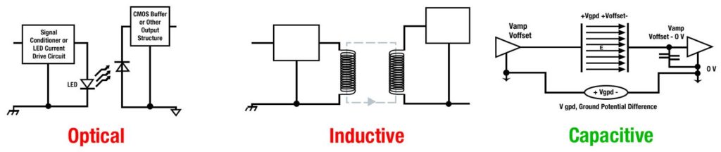

Figure 3: Electrical isolation types. Source: IEEE GlobalSpec
Galvanic isolation is most often used for one of two primary purposes. First, it provides safety for users of systems with potentially dangerous high internal voltages by assuring that these cannot reach the user despite any internal failures. Second, it enables a large class of innovative power-system architectures in which the primary and secondary sides must have no possible common current flow between them, such as when one side is ground referenced while the other side is “floating” with no ground connection.
The need for isolation is driven by a wide array of situations such as factory automation with extensive human/machine interfaces (HMI), solar panels and medical instrumentation. The higher dV/dt ratings of GaN and SiC power devices also drive challenging isolation requirements.
Trends related to isolation: Isolation can be solely for power rails, signal lines (data) or both. Ideally, IC vendors could put both power and data isolation in the same package for safety and reliability. Additionally, integrating both data and power isolation allows the IC vendor to better control, and design for, strict EMI standards typical in these applications.
The isolation level needed is a function of the application: a 5 kV reinforced isolation is adequate for many cases and there are detailed industry standards that define it.
Using isolation capacitors for data transfer is a popular approach due to superior common-mode transient immunity (CMTI) performance and data integrity. However, capacitive isolation is not viable for most power transfer applications due to the limited amount of power that can be transferred, along with the efficiency. Magnetic approaches are therefore the preferred choice when power transfer is required. Combining both approaches enables solutions such as fully “self-biased” transceivers with both isolated power and data connections in the same package. These kind of product and technology innovations truly change the game in these safety-critical applications.
Conclusions
Progress in power functions, components and delivery is interdisciplinary, as density, EMI and isolation are all closely related. For example, reduced EMI leads to reduced passive filter size, which leads to higher power density. Progress will come from “stacking” innovations leading much more major technology advances. Among these are availability of fully characterized wide bandgap (WBG) power devices, improved thermal interfaces for device die, increased integration of passive devices and functions, development of leading-edge process technologies and innovative circuit IP.
Texas Instruments, as a leading vendor of power-related components and design-in support tools, is developing technologies to enable and support these trends, including materials, processes, topologies, circuits and packaging.

