
source: ASRC AS&D at NASA Goddard Space Flight Center; ESA SPCD 2018 Symposium
EPCI e-symposium library article
Bulk metal foil and thin film resistors occasionally contain localized defects within the etched resistor pattern. Such defects are prone to fracture due to thermo-mechanical fatigue during powered operation, however common screening methods are not always effective at removing devices with such defects. An improved method has been developed to screen for localized resistor pattern defects. The method involves the application of brief, high power electrical pulses at a low duty cycle while inspecting the resistor with a high resolution, high speed infrared camera.
published by EPCI under approval of ESA SPCD 2018 organizing committee.
Title: A Screening Method Using Pulsed-Power Combined with Infrared Imaging to Detect Pattern Defects in Bulk Metal Foil or Thin Film Resistors
Author(s): Jay Brusse (1), Lyudmyla Panashchenko (2)
Organisation(s): 1) ASRC AS&D at NASA Goddard Space Flight Center Code 562 Greenbelt, MD 20771, USA 2) NASA Goddard Space Flight Center Code 562 Greenbelt, MD 20771 USA
Symposium: ESA SPCD 2018
Reference: Test, Reliability & Evaluation for space 1.
ISBN: N/A
e-Sessions Applications: Aerospace
e-Sessions Scope Components: Resistors
e-Sessions Topics: Quality & Reliability, Measurement & Test
INTRODUCTION
Bulk metal foil and thin film resistors occasionally contain localized defects within the etched resistor pattern. Common defects of this type include in-line constrictions referred to as notches, unremoved resistor material bridges between adjacent pattern lines, and embedded non-conductive particles in the resistor material. Such defects are prone to fracture due to thermomechanical fatigue during powered operation, especially power cycling, resulting in positive resistance change and open circuit failure modes. Common screening methods of optical microscopy, short time overload power tests (e.g., 6.25x rated power for 5 seconds) and burn-in (e.g., 1.5x rated power for 100 hours) are useful, but they are not always effective at removing devices with such defects.
An improved method has been developed to screen for localized resistor pattern defects. The method involves the application of brief, high power electrical pulses at a low duty cycle while inspecting the resistor with a high resolution, high speed infrared camera. The following test conditions were found to be suitable for this purpose: 6.25x rated power, 1 to 5 pulses, 50 ms pulse width and 10% duty cycle. During the power pulsing, localized constrictions in the resistor pattern are identifiable as hot spots via the infrared camera. Reject criteria can be established based on observations of hot spots.
To assess its effectiveness, a total of two hundred eighty (280) surface mount foil resistors (40 each from 7 different lots) were screened using this infrared technique. The screening identified twenty-nine (29) resistors with significant hot spots in the resistor pattern. All 280 resistors were then subjected to an industry standard 10,000 hour life test at 1x rated power at 70°C with power cycled for 90 minutes on and 30 minutes off. During life testing, three resistors exhibited positive resistance change failure mode. All three failures were due to thermomechanical fatigue failure of localized bridge defects at the locations identified via infrared screening. The results of this evaluation illustrate the benefits of the pulsed-power infrared detection screening technique to identify reliability suspect foil or thin film resistors that may escape common screening methods.
Traditional screening tests for resistors that might detect localized constriction defects include optical microscopy inspection of the resistor pattern prior to encapsulation or powered tests such as short time overload (STOL) and power conditioning (also known as burn-in) tests such as described in [1 – 3]. Experience has shown that despite the implementation of these screening tests, occasionally, some resistors with localized constriction defects will be supplied [4 – 8].
BULK METAL FOIL RESISTOR CONSTRUCTION
Surface mount foil resistors are commonly produced as two terminal devices with solderable wraparound terminations. They are available in a variety of standard footprints including sizes 0603 up to 2512 (see Fig. 1a). The basic construction of a bulk metal foil resistor is described in several patents [9, 10] and illustrated in Fig. 1 and Fig. 2 [7].
The typical surface mount foil resistor consists of a flat, rectangular, insulating substrate (e.g., alumina) on top of which the resistor element is bonded using adhesive materials (e.g., resins or polymers). The resistor element is made from proprietary nickel-chromium based alloy ingots that are precision-rolled into foil sheets having thicknesses in the range from ~2μm to ~5μm.
The foil sheets are then developed into serpentine resistor patterns using photolithography and electrochemical etching techniques. A wide assortment of resistor patterns may be produced with individual patterns having resistor lines (also called “gridlines”) having widths ranging from a few microns to many tens of microns depending on the resistance values to be achieved from that pattern.
Fig. 1b and 1c provide examples of the serpentine resistor patterns for a low value (49.9 Ω) vs. high value (20,000 Ω) resistor each produced on a size 1206 alumina substrate. The resistor pattern is comprised of a non-adjustable resistor section(s) plus a plurality of sections of various resistance values where each additional section has its own removable shorting tab connected to it in parallel.
The removal of a shorting tab (process known as trimming) is performed by the manufacturer using laser cutting, mechanical scribing or micro-sandblasting techniques. Removal of a shorting tab connects the associated previously-shorted resistor section in series with the remainder of the pattern thereby increasing the total resistance of the pattern by a fixed amount. By removing various combinations of shorting tabs, the resistor can be trimmed to any desired resistance value within a broad range and also achieve very precise tolerances (e.g., ±0.01%).
The resistor element is protected by a thin (~5μm to ~10μm), optically translucent polymeric coating followed by a thin (~25μm), optically opaque epoxy coating to protect the resistor element against handling damage and to allow for the printing of part markings (e.g., lot date code) onto the external surface of the component (see Fig. 2).
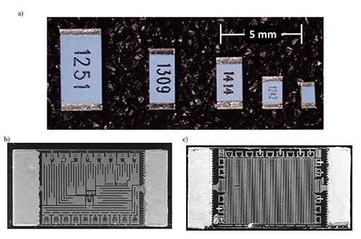

Fig. 1. a) Surface Mount Foil Resistors Sizes 2010 to 0603 Etched foil resistor pattern for size 1206 surface mount foil resistors b) 49.9 Ω and c) 20,000 Ω
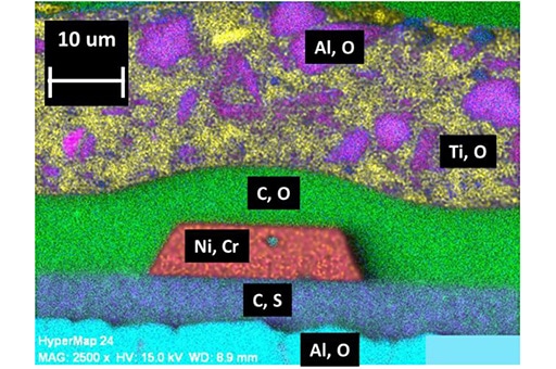
Fig. 2. Scanning Electron Microscopy (SEM) Image with Elemental Dot Map of a Cross Section of a Typical Surface Mount Foil Resistor
CONSTRICTION DEFECTS IN FOIL RESISTOR PATTERNS
Two main types of constriction defects may occur during the manufacturing of the foil resistor element: notches and bridges. Examples of each type of constriction defect are shown in Fig. 3 [4 – 8].
Notch defects are localized holes in the resistor gridline that reduce the gridline cross sectional area below the original design intent. Notches that take away >75% of the nominal resistor line width are considered to be unacceptable by some workmanship inspection criteria [3, 11] when the pattern is inspected at 30x magnification. The causes of notch defects include pre-existing pin holes in the foil sheet prior to etching, photolithography/etching-related anomalies and non-conductive particles (e.g., aluminum nitride) embedded in the foil [5]. If a notch defect breaks, then the electrical continuity of the gridline pattern is interrupted usually resulting in an open circuit failure mode. If the disrupted section of the resistor pattern has an associated parallel pathway, then a positive resistance shift occurs.
Bridge defects, as the name suggests, are sections of foil resistor material that interconnect two or more adjacent gridlines. Bridges whose narrowest width is <10% of the nominal resistor line width are considered to be unacceptable [3, 11]. The primary causes of bridge defects are related to photolithography/etching anomalies that result in a failure to completely remove foil material from the spaces between adjacent lines as intended. Bridges form unintentional parallel resistor pathways within the serpentine pattern. If during the trimming operation the manufacturer cuts a shorting tab associated with a section of the pattern containing bridge defects, then these bridges and the parallel resistance pathways they produce become essential features of the overall resistance value. Any disruption of the bridge would result in removal of the parallel path and an associated increase in resistance value.
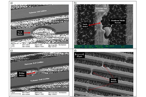
Fig 3. Destructive Physical Analysis (DPA) Examples of Constriction Defects in Foil Resistors
a) Large Notch Defect in Gridline,
b) Notch Defect Associated with an Aluminum Nitride Particle Embedded in the Foil,
c) and d) Bridge Defects Between Adjacent Gridlines
DESCRIPTION OF A NEW PULSED-POWER INFRARED SCREENING TECHNIQUE
With support from the NASA Electronic Parts & Packaging (NEPP) Program the authors have developed a new screening technique for foil and thin film resistors that is intended to augment the traditional testing methods. This new technique was initially described in our previous publication [12]. The primary objective of this technique is to identify and remove from the lot any resistors having significant localized constriction defects (notches and/or bridges) within the active region of the resistor pattern.
The technique is based upon the principal that significant constrictions will exhibit substantially greater Joule heating during powered operation compared to segments of the resistor pattern with the intended cross sectional area. The increased Joule heating results in the formation of localized hot spots in the resistor pattern which may then be detected by infrared thermography if the infrared detector has sufficient resolution.
….
infrared inspection was performed on several surface mount foil resistors and some surface mount thin film resistors while applying brief power pulses. Next figure provides a few examples of the kinds of pulsed-power infrared images obtained at this stage of development. The infrared camera’s software allows selection of a variety of color palettes to represent different temperatures within the field of view. For these images the green palette was chosen where darker colors are cooler and lighter colors are hotter. Note: Due to differences in the emissivity of the marking ink compared to the other materials, the part markings give a false impression of hotter temperatures at their location.
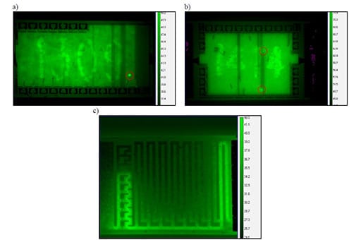
Fig.– Examples of Pulsed-Power Infrared Images of
a) Foil Resistor with a Notch Type Defect,
b) Foil Resistor with 2 Bridge Type Defects and
c) Thin Film Resistor with No Defects
EVALUATION OF THE NEW SCREENING METHOD
Having established the feasibility of the pulsed-power infrared screening method described above, an evaluation was performed to determine its effectiveness to non-destructively identify foil resistors having localized constriction defects and furthermore, to assess what, if any, effect such defects have on long-term reliability.
… continue reading the full paper in the link below.
CONCLUSIONS
Bulk metal foil and thin film resistors are occasionally produced having localized constriction defects (e.g., notches and bridges) within the active region of the etched resistor pattern. These types of defects have occasionally been observed to break in service (and during life test) due to the formation of localized hot spots that, especially during power cycling, result in thermo-mechanically-induced fatigue fracture.
The severity of failure depends on the type (notch vs. bridge) and location of the constriction in the pattern, but the failure mode is always a positive resistance change up to and including open circuit failure. Resistance shifts due to fracture of constriction defects can be permanent or intermittent. Intermittent resistance changes may occur if the fractured constriction defect undergoes displacements sufficient to make or break contact between the severed ends. Past experiences with this type of resistor include intermittent failures which abruptly, repeatedly and reversibly changed resistance at particular ambient temperatures.
Traditional resistor inspection techniques such as pre-encapsulation visual inspection, short time overload (STOL), power conditioning, and lot sample workmanship inspection via DPA can identify many resistors with constriction defects, but they do not remove all resistors with constrictions that may fracture in service. To augment these traditional inspections, a new screening inspection technique has been developed using a FLIR SC8300 high speed, high resolution infrared camera and 4x lens while applying 1 or more brief power pulses (e.g., 50ms @ 6.25x rated power) to the resistor under test. Resistors with significant localized constriction defects in the resistor pattern exhibit hot spots during this infrared inspection. Feature sizes below 5μm are readily detectable with this technique.
A conservative rejection criteria is to remove from the lot any resistor that exhibits a hot spot. This technique has been demonstrated to be usable as a non-destructive, post-procurement screening inspection on surface mount foil resistors and thin film resistors where the specific coatings used to protect the resistor element are highly transmissible in the spectral range of the infrared detector employed. Ideally, this same technique could be incorporated as an in-process screening inspection by a resistor manufacturer after resistor trimming to final value and prior to
encapsulation.
To assess the effectiveness of this pulsed-power infrared screening technique, we obtained a total of 280 high resistance value surface mount foil resistors comprised of 40 resistors from each of 7 different production lots. All of the resistors were pre-screened by the manufacturer using 100% pre-encapsulation visual inspection of the resistor pattern followed by either 1 or 2 exposures to STOL to remove as many defective resistors as these tests may detect. Next, the pulsed-power infrared inspection test described herein was performed during which 29 resistors were identified with significant hot spots associated with 1 or more notch and/or bridge defects in the resistor pattern. Resistors with hot spots were found at approximately the same rates of occurrence in each of the 7 lots regardless of the level of manufacturer pre-screening (e.g., 1 vs. 2 STOL exposures).
After the infrared screening test, all 280 resistors, including those with hot spots, were subjected to an industry standard 10000 hour life test at 1x rated power at 70°C with power cycled on for 90 minutes and off for 30 minutes. During the life test 3 resistors with significant hot spots prior to life test exhibited one or more positive resistance shift failure modes ranging from ~4000 ppm to ~19000 ppm detected after 250, 2000 and 4000 hours. Post-life test infrared inspection revealed that 1 or 2 pre-life test hot spots had disappeared from each of the 3 life test failures. The 277 resistors that passed life test all exhibited no changes in their infrared signatures before vs. after life test.
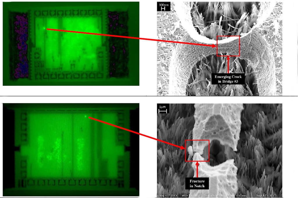
The 3 life test failures plus a few additional resistors that passed life test were then subjected to destructive analyses using a two-step chemical and plasma etching deprocessing scheme to remove the protective coating materials. High magnification inspection using SEM and EDS confirmed that each of the 3 life test failures had either 1 or 2 previously-conducting bridge defects that fractured at the approximate mid-point in their span producing an open circuit condition in the bridge.
Each fractured bridge resulted in the removal of a parallel resistance pathway in the resistor pattern thus producing the observed positive resistance shift failure modes. Detailed inspection of the fractured bridges showed no evidence of melting nor tensile stretch-to-break failure of the bridge. Instead, the fractures are consistent with cyclical fatigue fracture. It is concluded that the repetitive on/off power cycling during life test resulted in localized, thermomechanical expansion and contraction of the bridge defects (i.e., one expansion/contraction per on/off power cycle) that eventually caused the bridges to fracture.
SEM analyses of resistors with significant hot spots that passed life test showed evidence of emerging and/or near-complete fracture of their constriction defects. Since continuous resistance monitoring was not used during life test, it is possible some of these resistors exhibited intermittent resistance changes resulting from small displacements between the fractured ends of the constrictions causing them to make and break pressure contact between the fractured ends.
For applications requiring the highest reliability foil or thin film resistors, the authors recommend the use of the pulsed-power infrared screening technique described herein. This test can be adapted as an in-process manufacturing screen or as a post-procurement screening inspection. Both approaches identify resistors with localized constriction defects in the pattern. This evaluation and prior field experiences have shown such constriction defects have the potential to fracture in service resulting in positive resistance shift failure modes up to and including open circuits.
ACKNOWLEDGMENTS
The authors wish to acknowledge the NASA Electronic Parts & Packaging (NEPP) program and Mike Sampson for supporting this research. Special thanks is given to Jacob Musel, Ori Sinkevich and Steve Phillips of Vishay Precision Group for providing foil resistors and life testing services for this evaluation. Gratitude is given to Tim Mondy, Alexandros Bontzos, Matthew King-Smith, Henning Leidecker and Jack Shue at NASA Goddard Space Flight Center (GSFC) for their support in the development and implementation of the pulsed-power infrared screening technique. We are indebted to Chris Greenwell, Ron Weachock and Nilesh Shah of ASRC AS&D at NASA GSFC for their failure analysis expertise.
REFERENCES
[1] MIL-PRF-55342H with amendment 5, “Resistor, Chip, Fixed, Film, Nonestablished Reliability, Established Reliability, Space Level, General Specification for”, Sept. 5, 2017
[2] Models 303133 through to 303138 (Ultra High Precision Surface Mount Chip Resistors, VSMP Z-Foil Technology Configuration), Vishay Precision Group Data Sheets, http://www.vishaypg.com/docs/63169/30313x.pdf
[3] MIL-PRF-55182H with amendment 3, “Resistors, Fixed, Film, Non-established Reliability, Established Reliability, And Space Level, General Specification For”, Appendix B, para. B.7.2, April 8, 2009.
[4] NASA GSFC Code 562 Failure Analysis Report J17534FA, draft March 2018.
[5] NASA GSFC Code 562 Failure Analysis Report Q80471, March 6, 2009.
[6] NASA GSFC Code 562 Evaluation Report Q80487, March 13, 2009.
[7] NASA GSFC Code 562 Evaluation Report Q80490, April 3, 2009.
[8] NASA GSFC Code 562 Evaluation Report J12427, April 26, 2013.
[9] U.S. Patent 3,405,381, “Thin Film Resistor”, Oct. 8, 1968, Felix Zandman, Branin Boyd, Vishay Intertechnology, Inc.
[10] U.S. Patent 4,378,549, “Resistive Electrical Components”, Mar. 29, 1983, Joseph Szware, Ramat Gan, Vishay Intertechnology, Inc.
[11] MIL-PRF-1580B with change 3, “Destructive Physical Analysis for Electronic, Electromagnetic and Electromechanical Parts”, para. 18.4.3, March 4, 2014.
[12] L. Panashchenko, J. Brusse, M. King-Smith, “A Screening Method Using Infrared Imaging to Detect Pattern Defects in Foil and Thin Film Resistors”, 2015 Components for Military and Space Electronics (CMSE) Conference and Exhibition, Los Angeles, CA, March 1-3, 2015.
[13] FLIR SC8000 series data sheet, http://www.flirmedia.com/MMC/THG/Brochures/RND_018/RND_018_US.pdf


