06/02/2017 by Paul Pickering, Technical Contributor
Any discussion of plagues and parasites brings to mind thoughts of locusts, frogs, and biting insects. Thankfully, such events are rare in 2017, but if you work with high-speed digital and analog circuitry, there’s one sure way to risk a disaster of Biblical proportions: forgetting that the printed circuit board (PCB) is much more than a benign way to hook up your components.
As we all learned in school and (if you’re like me) promptly forgot, when frequencies increase, a PCB becomes anything but harmless. In fact, it’s then a component in its own right: a complex passive network of parasitic resistors, inductors, and capacitors that can wreak havoc with marginal designs.
The PCB As A Passive Network
PCB parasitics include inductors formed by package leads and long traces; pad-to-ground, pad-to-power-plane, and pad-to-trace capacitors; interactions with vias, and more.
Figure 1: The equivalent circuit per unit length of a PCB trace contains resistive, inductive, and capacitive elements. (Source: electronics.stackexchange.com)
Models are a good way to simulate the electrical contributions of PCB parasitics. Figure 1 shows the basic block of the distributed element model (transmission line model) of a PCB trace: R, L, and C are exactly what you’d expect; G is the conductance of the PCB dielectric.
Quantifying PCB Parasitics
How can we get an idea on the magnitude of these PCB parasitics? Let’s start with trace resistance.
The standard PCB uses 1-oz copper traces, which have a thickness equal to one ounce of copper evenly spread over a one square foot area, or 1.37 thousandths of an inch (mils). The 1-oz copper has a resistivity of ~ 0.5 mΩ per square, which equates to 5 mΩ for a 10-mil trace per 100 mil of length.
Since most low-power designs do not carry more than a few milliamps of current, the effect on trace resistance is often negligible. For high-current paths, though, even a few milliohms can cause voltage drops and excessive temperatures, calling for wider traces.
PCB capacitance and inductance pose greater problems because they can couple RF voltages and currents into nearby traces and reduce the effectiveness of decoupling capacitors and EMC filters.
The dimensions of a trace or via, plus the relative permittivity, εr, of the PCB material, determine its inductance and capacitance. FR-4 glass-reinforced epoxy, the most common PCB material, has an εr range from 4.0 to 5.0: 4.5 is often used as a typical value.
Figure 2: The formulas for calculating trace inductance and capacitance. (Source: Texas Instruments)
The formulas for PCB inductance and capacitance are complicated: the ones given in Figure 2 and 3 are approximations. A 0.8 mm (0.031”) trace on a 0.8 mm (0.031”) thick FR-4 PCB, for example, has about 4 nH inductance and 0.8 pF capacitance per cm, or ˜ 10 nH and 2.0 pF per inch.
Figure 3: The equivalent formulas for vias. (Source: Texas Instruments)
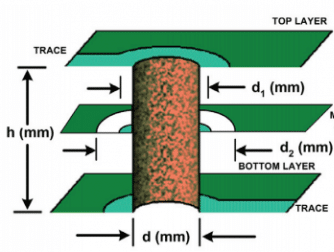
A different set of approximations applies to PCB vias—connections that route signals between different PCB layers.
Applying the equations in Figure 3, a 0.4 mm (0.0157”) via through a 1.6 mm (0.063”) PCB has ˜ 1.2 nH inductance; even the clearance hole can contribute some parasitic capacitance.
Since the length of a via is typically very small relative to the rest of the trace, its contribution is often ignored. This can cause issues, though with very high frequency (>100MHz) signals, or in situations where the high-frequency harmonics contain significant energy.
To save you ploughing through the math, help is available online. The Vehicular Electronics Laboratory at Clemson University, for example, offers online calculators for several transmission methods including surface microstrips, embedded microstrips, and striplines.
Some Effects Of PCB Parasitics
PCB parasitics cause problems in a variety of areas. In a switching power supply—a synchronous buck converter, for example—parasitic inductance can slow down the turn-on and turn-off time of the power FET and increase switching losses.
Figure 4: In a synchronous buck converter, the internal and external inductances in the source path of the HS FET combine to form the common-source inductance (LCSI). (Source: EEWordsmith)
As Figure 4 illustrates, the inductances of both the PCB trace and the FET’s internal bond wires contribute to the total inductance between the HS FET source and the gate driver return path.
Both the (high) drain-source current and (low) gate-charging current flow through the common-source inductance. A change in IDS will induce an opposing voltage VCSI in LCSI, and modify the gate-source voltage VGS seen by the power MOSFET. The effect is an increase in FET turn-on and turn-off times, resulting in increased switching losses.
Parasitics can also change the performance of high-speed analog designs. Figure 5 shows a typical op amp circuit as it appears on the schematic, and real-world circuit on a PCB; every pad adds a parasitic capacitor, and every trace adds a parasitic inductor. Just for fun, resistors, capacitors, and inductors are far from ideal and each one adds its own set of parasitics to the mix.
As little as one pf of unwanted parasitic capacitance at the inverting input of an op amp can cause an additional 2 dB of gain at high frequencies; a few nH of added inductance from a two-inch trace can result in a low-level oscillation.
Figure 5: (a) A typical op amp design schematic, and (b) the design with parasitics included. (Source: Analog Devices)
Digital designs aren’t immune, of course. The latest USB 3.1 SuperSpeed+ specification allows for data rates of 10 Gbps; HDMI 2.1 has four data lanes, each running at 12 Gbps.
At these speeds, it’s critical to maintain impedance matching throughout the signal path. Any mismatch caused by PCB parasitic capacitance will cause reflections on the line, increase jitter, and compromise signal quality.
General Guidelines For Reducing The Effects Of Parasitics
Paying close attention to PCB layout can go a long way in reducing parasitics. Manufacturers of high-speed analog and digital circuits offer numerous application notes, tutorials, and seminar material on PCB layout best practices: the information from Texas Instruments and Analog Devices is particularly instructive. For digital circuitry, Howard Johnson and Martin Graham have written a well-regarded book on high-speed digital design, appropriately subtitled A Handbook of Black Magic that covers many of these topics.
IC suppliers can help reduce the effects of PCB parasitics, too.
In the digital arena, devices placed in the high-speed data path often employ “flow-through” packaging that helps keep the trace lengths equal between the positive and negative lines of the differential data lanes to avoid impedance mismatch.
In power ICs, manufacturers are working to reduce the effects of internal parasitics from such items as bond wires and pins. Texas Instruments, for example, offers its PowerStack technology that places two NexFET power transistors directly on top of each other in a three-dimensional package; this arrangement virtually eliminates resistance and parasitic inductance between the FETs. In a synchronous buck converter, that translates to lower common source inductance, resulting in lower switching losses and higher efficiency.
Conclusion
There’s a popular quote, usually (though erroneously) attributed to Mark Twain: “It ain’t what you don’t know that gets you into trouble. It’s what you know for sure that just ain’t so.”
Paying attention to the effects of the PCB on your high-speed design will not only keep you out of the second category, it might also avoid a plague. In this case, of late nights, lost weekends, and angry bosses.
Best of luck with the frogs and the rest. Although I do like a plate of cuisses de grenouille now and then. Locusts, not so much.