
This article elaborates on design and calculation of Flyback DC/DC converters. The post is based on Würth Elektronik‘s “DC/DC Converter Handbook” that can be ordered from WE website here. Published under permission from Würth Elektronik.
Key Takeaways
- This article discusses the design and calculation of Flyback DC/DC converters, emphasizing their efficiency and cost-effectiveness.
- Flyback converters work well for isolated, regulated output voltages up to 150 W, using fewer components to reduce costs and size.
- It covers input and output filter designs, EMC considerations, and capacitor selection for optimal performance.
- The article includes example calculations for a Flyback converter with specified input and output parameters, ensuring proper performance under load.
- Common mode and differential mode interference is addressed, along with solutions for mitigating emissions in practical applications.
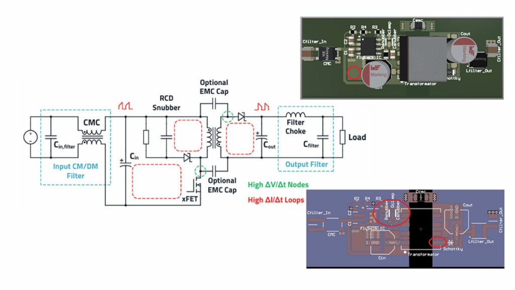
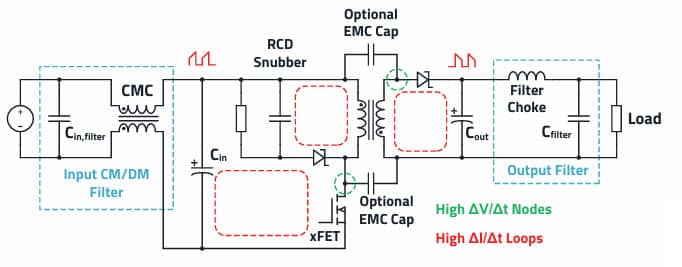
Flyback Converter Block Diagram and General Thoughts
If one or more isolated, as well as regulated output voltages are needed, then the flyback converter up to approximately 150 W is often the best choice. This is mainly due to the fact, that it requires relatively few components, thus keeping the costs and space requirements low. You can see an overview of basic power converters in the article DC-DC Converter Basic Characteristics and Formulas.
At higher power levels, other topologies, such as the forward converter, are advantageous because they also make better use of the transformer’s core volume. The flyback converter has trapezoidal discontinuous current curves at the input and output through the respective capacitors.
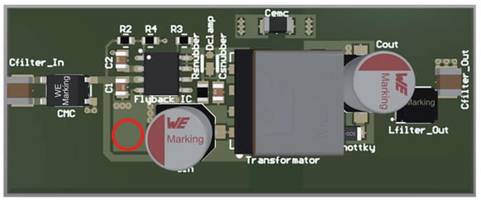
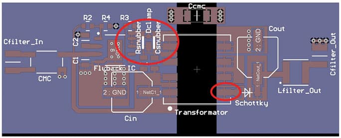
In practice, two EMC filters (see Figure 1.) are therefore often necessary. As this converter has an isolated topology, common mode currents must also be increasingly expected above the switching frequency. This largely comes from the transformer’s parasitic coupling capacitance between the primary and secondary sides. Because of the high ΔV/Δt of the primary switching node (the hot node), a dielectric displacement current is superimposed on the secondary side via this coupling capacitance, which then flows via the ground (GND) to the primary side and during the EMC measurement of the interference voltage, via the LISN.
Common mode currents are also generated when an external MOSFET is used, and it is mounted on a heat sink or other metal surfaces. A parasitic capacitance arises between the MOSFET and the heat sink in this case, over which a dielectric displacement current also shows up. Many flyback applications
therefore use current compensated chokes in the input filter, as well as Y2 safety capacitors against ground. Capacitive current dividers can also be built from the primary to the secondary side with the help of the appropriate capacitors, which lead part of the common-mode currents back to the source by the shortest route. Should the application require reinforced insulation between input and output, Y1 capacitors must always be used for safety reasons. A downstream LC filter is often required to reduce the voltage ripple at the output. This filter also reduces interference up to approximately 30 MHz.
Example Flyback Converter Design and Calculation
Transformer for a flyback converter:
Input voltage: Vin = 24 V
Output voltage: Vout = 5 V
Output current: Iout = 5 A max.
Switching frequency: fsw = 300 kHz
Max. bandwidth control loop/crossover frequency: fc = 10 kHz
Forward voltage rectifier diode: VD = 0 V (this example is a flyback with synchronous rectifier)
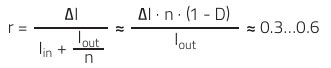
Ripple current factor:
Data sheets for flyback transformers often contain specific application recommendations. This means that the transformer was specifically developed for a particular application, which does not necessarily mean that it is unsuitable for other boundary conditions. But it is expedient if the application recommendation is already close to the target application.
Unlike the topologies already discussed here, it is quite common in flyback design for the ripple factor to exceed 200%. This is the case for a flyback converter operating in discontinuous mode (DCM). Especially in AC/DC applications, the associated high peak currents are accepted in order to benefit from the reduction of switch-on losses (due to currentless switch-on) and the simplified transformer design.
The fastest and easiest way to get there for DCM, Quasi-Resonant or Boundary Mode designs is to use the REDEXPERT flyback transformer selector tool.
Other mathematical relationships apply to a flyback in discontinuous operation, which are not dealt with here.
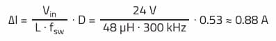
In order to have a wider choice of transformer inductance, the usual range of 0.3…0.6 is chosen for the ripple factor, rather than specifying a certain ripple factor.
Unlike the case of non-insulated topologies, before the inductance is defined, the turns ratio n must be defined.
The turns ratio is directly related to the duty cycle D. To avoid high peak currents during demagnetization of the transformation (blocking phase), it is beneficial to keep the duty cycle below 60%. The duty cycle may also be limited by the controller IC used; duty cycles of 50…80% are common.
Turns ratio n:
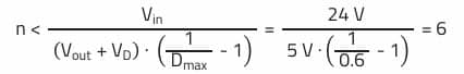
In many AC/DC applications, the maximum drain-source voltage of the primary-side MOSFET can also be the limiting factor for the turns ratio, as the turns ratio increases the transformed output voltage to the primary side during the blocking phase.
The WE portfolio includes the article WE-PoEH (749119550), which has a turns ratio of 5.33 (primary/secondary), relatively close to the maximum envisaged value of 6. According to the application recommendation, an output current of 2…3 A at 5 V can also be achieved. If the two secondary windings (N2, N3) are connected in parallel, a maximum output current of 6 A can be expected. Although the application recommendation deviates slightly regarding the input voltage (recommendation: 33…57 V), this is not considered critical due to the low winding resistance of the primary winding (70 mΩ) and the sufficient saturation current margin (see Isat).
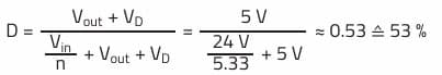
Duty cycle D:
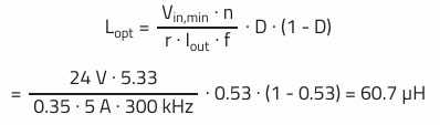
Optimal primary inductance value lopt:
Considering a transformer inductance value of 48 µH (WE-PoEH 749119550), this results in a ripple current of:
Ripple current factor r: The selected transformer thus also defines the ripple current factor.
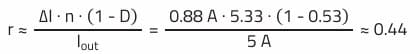
Thought higher than the typical starting point of r = 0.35 because of the lower inductance, at 0.44 (44%), this is well within the target range of 0.3…0.6.
Saturation Current Isat:
Half of the AC ripple current must be added to the average current during the on-phase to obtain the maximum peak current in the primary winding. Due to the functional principle of the flyback converter, current flows in the primary winding only in the on-phase.
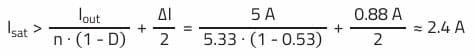
The saturation current of the WE-PoEH (749119550) transformer is specified as 3.6 A. There is sufficient margin and core losses should remain moderate. Input capacitor for a flyback converter.
Selection of the specific input capacitor for just this application is explained in detail in article: Selection of Capacitors for DC/DC Converters.
RMS current through the input capacitor:
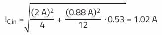
Using the REDEXPERT tool, the capacitor WCAP-PTHT (870135675003), a 100 µF/35 V polymer aluminum capacitor, was selected as the input capacitor. The capacitor has a small impedance at the switching frequency of 300 kHz while meeting the requirements for ripple current and voltage.
Output Capacitor for a Flyback Converter
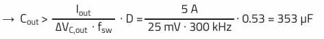
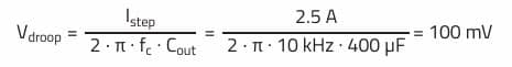
The output capacitor is defined based on the maximum permissible voltage ripple and on the basis of the maximum permissible voltage change (Vdroop) resulting from a load step. In our example we want to achieve a voltage ripple of 1% (50 mV) at an output voltage of 5 V. The voltage change must not exceed 3% (150 mV) for a load step from 2.5 A to 5 A (Istep = 2.5 A). From these assumptions, the minimum necessary capacitance can be calculated, which fulfills both requirements.
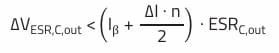
For the output voltage residual ripple, in addition to the capacitance-dependent part, the influence of the ESR is considered (the ESL is neglected). For simplicity, an even split is assumed for the two components, resulting in 25 mV each for the capacitance and the ESR calculations. With the flyback, the extent to which this addition actually occurs depends on the duty cycle and the magnitude of the ripple current.
In addition, it must be checked mathematically whether the AC current through the output capacitor stays below the maximum ripple current according to the datasheet.
Output voltage ripple:
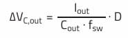
Minimum required output capacitance:
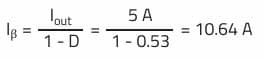
Average current through Cout:
Output voltage ripple due to ESR of the output capacitor:
Maximum allowed ESR of the output capacitor:
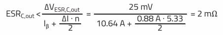
Output voltage droop during load step:
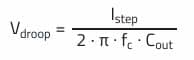
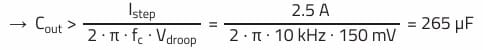
Minimum required output capacitance to cover max. allowed voltage droop during load step:
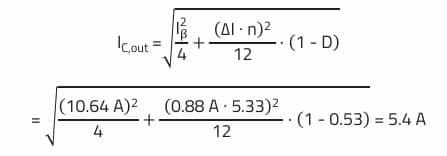
RMS current through the output capacitor:
The capacitance of 265 µF is not relevant in this case, as the minimum necessary capacitance of 353 µF results from the ripple requirement. Based on the results, we therefore need a capacitor with at least 353 µF and an ESR lower than 2 mΩ at 300 kHz.
As already described in Selection of Capacitors for DC/DC Converters, more than one output capacitor must be considered be cause of the high RMS current of 5.39 A.
In this design, a parallel connection of four aluminum polymer WCAP-PHGP capacitors with part number 875015119003 was used. The four polymer SMT capacitors (each 100 µF/6.3 V) have a combined total capacitance of 400 µF with a theoretical ESR of 1.7 mΩ at 300 kHz.
Considering the reduction factors a = 0.8 for the uneven current distribution (impedance deviation) and b = 0.8 at 300 kHz for the frequency dependency of the ripple current, according to REDEXPERT there is a permissible ripple current of approximately 13 A for the four capacitors (m = 4).

Therefore, sufficient margin exists for the calculated current through the output capacitors of 5.39 A.
The following output voltage waveform vC,out(t) was measured in the application:
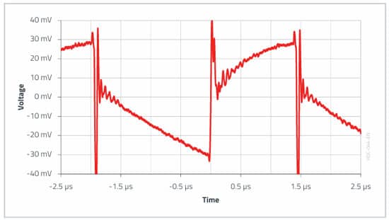
This voltage waveform was recorded with the oscilloscope given a bandwidth limitation of 20MHz and a very short ground contact via a probe spring directly on the last output capacitor. This is a common procedure in ripple measurements to keep parasitic effects low, which occur as superimposed high-frequency oscillations in the ripple measurement.
Neglecting the ESL voltage spikes, the measured ripple of approximately 60 mV is still above the design specification of 50 mV. This is mainly thanks to the fact that the layout and the solder connections of the capacitors result in additional parasitic impedance, which makes the total impedance higher than expected.
An additional LC output filter can help, whereby a ripple of 60 mV should not be critical for most electronic circuits.
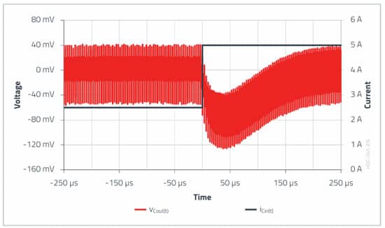
With a 2.5 A load step, the voltage change of approximately 75 mV (ripple not included in the analysis) is even lower than would be expected theoretically.
This is mainly due to the strong closed-loop simplification that forms the basis of this equation. The influence of the phase margin on the load step change is completely neglected (assumption: φm = 60°).
At this point, the advantage of SMT polymer capacitors should be highlighted, which retain their capacitance even under voltage load, in contrast to MLCC capacitors. This is a great advantage, especially for load step buffering.
Input Filter for a Flyback Converter
Before sizing the specific filter elements below, it helps to see how these EMI component families relate to each other:
| EMI / Filter Component | Position | Primary Function | Selection Highlights |
|---|---|---|---|
| Common mode choke | AC input, DC input or output lines | Suppress common mode conducted noise | Core material for frequency range; leakage inductance; current rating; safety approvals |
| Differential mode choke | Input filters, DC bus filters | Attenuate differential mode noise and ripple | Inductance vs. current; saturation; copper and core losses; temperature rise |
| X capacitors | Across AC lines | Reduce differential mode noise on mains | Safety class (X1/X2); surge handling; self-healing film types |
| Y capacitors | Line to earth | Reduce common mode noise within leakage current limits | Safety class (Y1/Y2); leakage current; creepage and clearance; insulation system |
Source: Passive Components for Power Converters Dossier, Passive Components Blog.
As mentioned in this article, flyback converters can also be expected to increasingly cause common-mode interference above their switching frequency. In contrast to the differential-mode interference calculated in Selection of Capacitors for DC/DC Converters for exactly this application, in practice it is difficult to determine the common mode interference in advance. Here there is a lack of knowledge of the effective parasitic coupling capacitance. This depends not only on the actual flyback converter but also on the load supplied.
Generally, it is expedient to use REDEXPERT to select a current-compensated choke that has the highest possible common-mode impedance at the dominant common-mode interference frequency (e.g., switching frequency) and its harmonics.
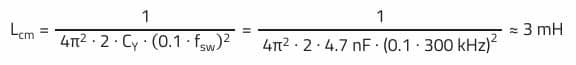
If it is also possible to use Y-capacitors in the application, the common-mode filter effect can be increased considerably. In practice, the size of Y-capacitors is limited by the permissible leakage current to ground (residual current). Typical values are up to 4.7 nF. Although the limitation due to leakage current generally does not apply to the DC example application, certified Y2 safety capacitors, such as the WCAP-CSSA series, are still beneficial. They withstand the pulse voltage that occurs, for example, during the surge test line to earth (+/L or –/N to PE).
If Y-capacitors are used, Thomson’s oscillation equation according to Input filters for DC/DC converters can also be applied to the common mode input filter. It is also a prerequisite that the Y-capacitors are placed behind the common-mode choke toward the common-mode interference source (in the direction of the DC/DC converter). This is also due to the fact that the impedance conditions are distributed differently in common mode than in differential mode. The interference source impedance corresponds to the parasitic capacitance from the switching node to ground.
For example, a 10 pF parasitic coupling capacitance at 10 MHz interference frequency gives approximately 1.6 kΩ. This is contrasted by the common-mode impedance of the line impedance stabilizing network – resulting from the parallel connection of the two measurement channels with 50 Ω impedance – with a total of 25 Ω. Assuming that two (+/L-ground, –/N-ground) 4.7 nF Y-capacitors (4.7 nF/250 VAC, WCAP-CSSA 8853522140011) are used, the necessary common-mode inductance of the common-mode choke for 40 dB attenuation is calculated as follows:
For the application, a common mode choke with slightly less rated inductance was selected using REDEXPERT with article WE-CMB S-Type 744822222 (L = 2.2 mH, IR = 2 A). This keeps the winding losses lower than with the 3.3 mH choke in the same design. In addition to the rated inductance, the common-mode impedance curve of the choke should also be considered. The self-resonant frequency of the common-mode choke – which results from the inductance and
the parasitic winding capacitance – represents another cut-off frequency for the common-mode filter, which directly limits the maximum attenuation. In the common-mode impedance curve, the self-resonant frequency corresponds to the frequency at which the impedance maximum is attained.
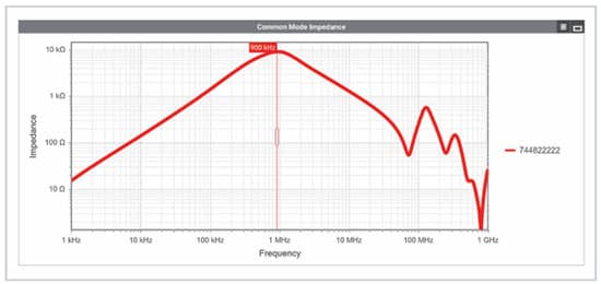
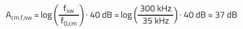
According to Figure 5. from REDEXPERT, the self-resonant frequency of the selected choke is approximately fres,cmc = 900 kHz. Now the maximum common-mode attenuation of the filter Acm,max can be calculated in decibels (assumption: ideal 2nd order filter):

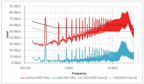
The common-mode attenuation at the switching frequency is theoretically:
The following improvement was achieved with the selected CM filter in the common-mode interference spectrum of the example application in Selection of Capacitors for DC/DC Converters.
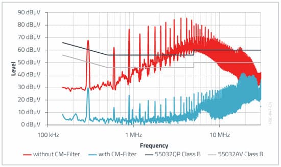
For higher frequencies (>5 MHz), the theoretical maximum common-mode attenuation is no longer achieved. The reasons behind this are the impedance conditions changing with increasing frequency, an increasing differential-mode/common-mode conversion, as well as increasing field-bound effects.
It has already been shown in Selection of Capacitors for DC/DC Converters that the differential-mode interference in this application is also above the limit value. The necessary additional LC filter could be designed as explained in Buck Converter Design and Calculation. Another variant is to intelligently use the existingfilter element – the common-mode choke. The common-mode choke has a leakage inductance that acts in differential mode. For the WE-FCLP and WE-LPCC series, the leakage inductance is explicitly stated in the data sheet.
It is also possible to use the differential-mode impedance curve in REDEXPERT to determine the approximate magnitude of the leakage inductance Ls,cmc.
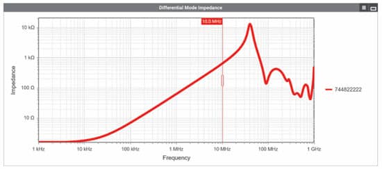
Using the cursor function, an impedance of 633 Ω can be determined in the inductive range of the differential-mode impedance curve at 10 MHz. This results in a leakage inductance of approximately 10 µH:
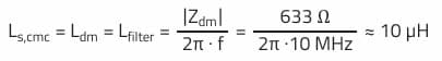
Given the filter inductance (leakage inductance), the required filter capacitance for 40 dB attenuation can be calculated:
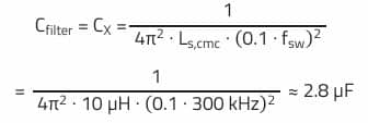
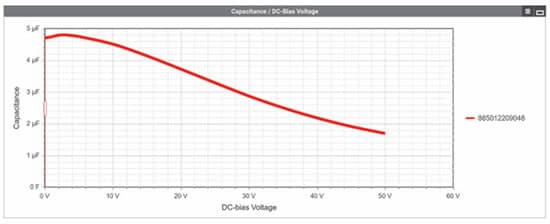
A MLCC ceramic capacitor (WCAP-CSGP 885012209048) with 4.7 µF/50 V and a 1210 package was selected for the filter. The higher capacitance value of 4.7 µF was chosen purposefully, on the one hand as a tolerance margin for the leakage inductance, and to compensate for the capacitance loss due to the DC bias effect, on the other.
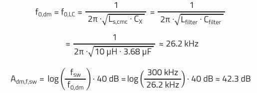
With the help of REDEXPERT, a remaining capacitance of 3.68 µF is determined at an input voltage of 24 V (DC bias) according to Figure 8.
This results in differential-mode attenuation at the switching frequency of:
The following improvement was achieved with the selected DM filter in the differential-mode interference spectrum of the application.
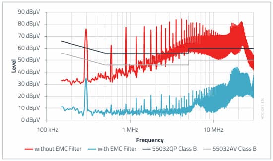
For the combined measurement per channel (see Figure 10.), the limit value for conformity with the standard is also reached by the filter.
Output Filter for the Flyback Converter
The dimensioning to reduce the output voltage ripple can be done according to the same principle as explained in the Buck Converter Design and Calculation. Another critical point can be the radiation of high-frequency common-mode interference via the load or connected periphery. PoE (Power over Ethernet) applications are a good example of this, where the PSE (Power Sourcing Equipment) is often designed as an isolated flyback converter. Without an additional common-mode filter at the output, amplified radiation often occurs from the Ethernet cable (antenna) of the common-mode interference generated by the flyback converter.
A good approach is to select a common-mode choke at the output that has the broadest possible impedance curve and whose impedance maximum is between 30 and 300 MHz. Depending on requirements, the upper conducted frequency range (5…30 MHz) or only the radiated frequency range (>30 MHz) should be covered. The problematic radiated interference caused by the switching operations of the power switches (e.g., reverse recovery of the rectifier diode) is usually between 30 and 300 MHz.
Read also the related articles in this series:
The same common-mode/differential-mode filtering logic — including a worked example for a compact QR/active-clamp flyback adapter and derating guidelines for each of these filter component families — is covered in more depth in our Passive Components for Power Converters Dossier.
- Causes of Oscillations in Flyback Converters
- Selection of Capacitors for DC/DC Converters
- Selection of Storage Inductors for DC/DC Converters
- Input filters for DC/DC converters
- Switching vs Linear Power Converters Compared
- Buck Converter Design and Calculation
- SEPIC Converter Design and Calculation
- Boost Converter Design and Calculation
- Fly-Buck Converter Explained and Comparison to Flyback
- LLC Resonant Converter Design and Calculation
- Calculating Resistance Value of a Flyback RC Snubber
- Flyback Transformer Understanding and Design
- Designing 800 V DC EMC Filters: Calculation, Simulation and Measurement – Flyback Converter Example
SEPIC and Flyback Converter Basic Formulas
The following table 1. provides basic formulas of the SEPIC and flyback converter topologies.
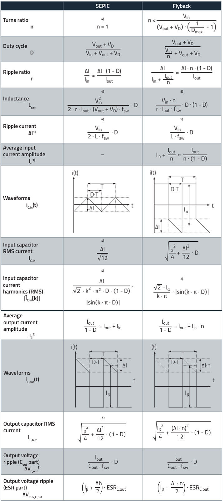
1) These assumptions apply to the ideal switching regulator in continuous conduction mode
(CCM), i.e., the efficiency of the converter is assumed to be 100% (η = 1).
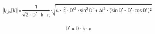
2) The current curve from this equation is approximately rectangular (ΔI neglected). Exactly:
3) The equations defined for ΔVC,out apply to the ideal capacitor. Cout therefore defines the minimum capacitance to meet the ripple voltage requirement. The actual voltage ripple will be higher due to the parasitic inductance ESL (equivalent series inductance) and ESR (equivalent series resistance) of the capacitor.
4) These equations only apply for a coupled choke with a turns ratio of 1:1 (n=1).
5) L corresponds to the main inductance (primary inductance) of the transformer.
Flyback Converter Design and Calculation – FAQ
A flyback converter is an isolated DC/DC converter topology commonly used up to 150 W. It is valued for its simplicity, low component count, and cost-effectiveness, making it ideal for applications requiring regulated and isolated outputs.
Flyback converters are best suited for low-to-medium power levels (up to ~150 W). For higher power levels, forward or resonant topologies are more efficient as they utilize transformer core volume better.
Key challenges include managing high ripple currents, ensuring proper transformer design, controlling EMI noise, and selecting suitable input/output capacitors and filters to meet ripple and stability requirements.
Due to transformer parasitics and switching behavior, flyback converters generate common-mode currents. Designers often use current-compensated chokes, Y-capacitors, and LC filters to reduce interference and meet EMC standards.
Simulation and selection tools like Würth Elektronik’s REDEXPERT assist in choosing transformers, capacitors, and chokes, while also helping to calculate ripple, inductance, and filter requirements.
How to Design a Flyback Converter Step by Step
- Define Input and Output Requirements
Specify input voltage, output voltage, maximum output current, and switching frequency. Example: Vin = 24 V, Vout = 5 V, Iout = 5 A, fsw = 300 kHz.
- Select Transformer and Turns Ratio
Choose a transformer with suitable inductance and turns ratio. Keep duty cycle below 60% to avoid high peak currents. Example: WE-PoEH 749119550 with 48 µH inductance.
- Calculate Ripple and Peak Currents
Determine ripple current factor (typically 0.3–0.6). Ensure transformer saturation current is above calculated peak current for safe operation
- Choose Input Capacitor
Select a capacitor with low impedance at switching frequency and sufficient ripple current rating. Example: 100 µF/35 V polymer aluminum capacitor.
- Select Output Capacitor
Dimension based on ripple voltage and load step requirements. Use parallel capacitors to handle high RMS currents. Example: 4 × 100 µF polymer capacitors.
- Design Input and Output Filters
Use common-mode chokes and Y-capacitors to suppress EMI. Add LC filters to reduce ripple and meet EMC compliance.
- Validate with Measurement
Measure output ripple and load step response with an oscilloscope. Adjust layout and add filters if ripple exceeds design targets.

