
Source: Alter Technology article
The cross-sectioning process provides access to the device internal structure, its materials and design. Such components as diodes and capacitors and silicon dice are often subjected to cross-sectioning to detect the defects which could not be found using other testing techniques.
Cross-sectioning generally involves three discrete steps: mounting the sample in a block of epoxy resin to form the specimen, grinding or cutting the specimen and finally polishing the surface so exposed. The main purposes of these steps are exposed hereafter.
Mounting:
- To hold the sample and their internal elements together during the sectioning process.
- To provide a means of holding the sample during grinding and polishing operations.
- To provide a convenient means of positioning the sample on the microscope stage for examination.
The purpose of grinding is to quickly reach the broad region of interest. This enables the exact area of interest to be reached by subsequent slower polishing techniques in a reasonable period of time. Grinding is carried out by using silicon carbide paper disks mounted on horizontal rotary grinding wheels. A continuous flow of water is used for cooling and cleaning the wheels.
doEEEt provides you the most complete and updated information about Hi-Rel EEE parts
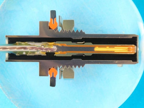
FIGURE: Cross-sectioned wired connector

The purpose of polishing is to eliminate surface scratches produced during grinding while maintaining sectioned sample features essentially unchanged so that a true view of these features is adequately available for visual inspection.
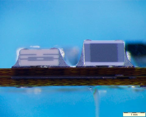
FIGURE: PCB cross-section with soldered ceramic capacitors

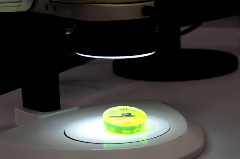
After fine polishing, the samples are examined microscopically using a compound microscope with vertical illumination to locate, identify and characterize defects which constitute reject criteria.
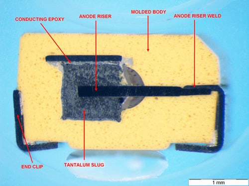

FIGURE: PCB cross-section of tantalum SMD chip capacitors
A key element in the performance of cross-section is the ability of the inspector to detect and identify problems and non-conformances of the products. Extensive experience in the technologies examined, knowledge about acceptance criteria and cumulated know-how are a prerequisite for proper test execution.
About Author
Francisco Javier Aparicio Rebollo is a Senior materials and Test Engineer at Alter Technology. Francisco Javier has a Degree in Physics and a Ph.D. in Materials Science both from the University of Seville and has conducted different Post-doctoral stays at the University of Mons (Belgium), University of Trento (Italy) and the Spanish National Research Council. He works as materials and physical test senior engineer within the Destructive and Physical Analysis Department. In Alter Technology laboratories, his main tasks address the characterization of EEE parts by advanced microscopy techniques and the conception of new test procedures.

