by Ciprian Ionescu, Andrei Drumea, Paul Svasta, Alexandru Vasile, Norocel Codreanu
University “Politehnica” of Bucharest, Romania, Center of Technological Electronics and Interconnection Techniques, UPB-CETTI
presented by C.Ionescu at the 2nd PCNS 10-13th September 2019, Bucharest, Romania as paper 5.3.
Abstract
Supercapacitors are strongly emerged as a promising technology to complement the batteries. Due to their low rated voltages it is usual to build supercapacitor banks, with series connection, in order to obtain higher voltage levels. Because of manufacturing dispersion parameters, during operation in multiple charge-discharge cycles it is very probable to result an uneven state of charge (SOC). During charging at constant current the capacitor that reaches first the rated voltage level could be damaged in a further charging process.
In order to prevent this, additional circuitry, named briefly, balancing circuit is provided. The balancing circuit with resistors and diodes are a simple solution, but with high power losses and modest performances. An improved solution is to use transistors to bypass the charging current, when an overvoltage is detected at each capacitor terminals. An even better solution is to use smart control using microcontroller or dedicated circuits for monitoring the series connection of supercapacitors.
We present in this paper our experience based on a dedicated integrated circuit. The circuit was developed by TI based on circuits already in use for Li ion batteries. The integrated circuit bq33100 [1] provides more than balancing of supercapacitor banks, being a single-chip solution that provides many features for charge control, monitoring, and protection of maximum 5 series capacitors. The circuit bq33100 can be programmed to determine periodically or at command the capacitance and equivalent series resistance (ESR) of the supercapacitor series group during normal operation. We will present the results that proved the effectiveness of balancing for a bank that uses 5 capacitors of 22F, starting from different SOC at each capacitor and for different charging currents. The test board built around the circuit is performant, energy efficient and can be further improved to ensure the balancing control for larger capacitance, by increasing the charging and bypass current.
Introduction in Capacitor Charge Balancing
The Supercapacitors or EDLCs are now seen as a promising energy storage alternative to batteries, but not only. A certain drawback of the supercapacitors is their low rated voltage. The usage in automotive applications at a rated voltage of about 14V requires a series connection, typical of six (or five) individual EDLCs’, usually called cells. In this way, the useful capacitance is reduced to C/6,(or C/5) see Fig. 1.

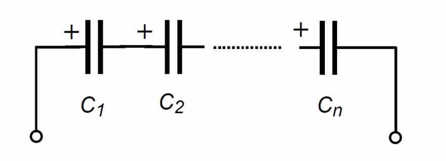
In order to increase the capacitance in a series connection it is necessary to construct a supercapacitor module (SM) using also parallel connections. This parallel connection is also useful to reduce the equivalent series resistance (ESR) of the module [2]. In a SM it is very probable that the SOC of each cell will be unequal in a real operation under load and multiple charge discharge cycles.
A cell that presents a higher capacitance will show a reduced SOC (or voltage). The uneven distribution will be more obvious during charging process. The charging process of series connected capacitors is affected by the non equal capacitance values. The EDLC as an electronic component is subject to inherent variation of parameters from device to device, for instance the capacitance, the leakage current or the ESR (Equivalent Series Resistance).
These differences in capacitance are caused by manufacturing variances or are caused by aging. The supercapacitor capacitance could vary up to ±20% of the rated value. This variance of capacitance can create a variation in the voltage of supercapacitor during the charge-discharge process (dynamic). Voltages of individual capacitors during a charging process with the current I0 can be written as:


(1)
with C1 to Cn the capacitance of the device 1 to n respectively.
During the pauses in charge-discharge process, the different values of the leakage current of capacitors can create a dispersion of the individual capacitor voltages (static), defined as:


(2)
where IL1 to ILn is the leakage current of capacitors 1 to n respectively.
And last but not lest, the variation that exists in the values of capacitor’s ESRs also creates some dispersion (dynamic) in the individual voltages when the supercapacitor series connection is submitted to charge- discharge process. The resulting voltages are:


(3)
where R1 to Rn is the ESR of the capacitor 1 to n respectively and I0 is the charging current.
From (1) can be seen that during charging with constant current, the capacitors with greater capacitance will be charged to lower voltages, and the capacitors with smaller capacitance will be charged to higher voltages. So, the voltage distribution is initially depending on capacitance values and when the charging was ended it is depending on the leakage current.
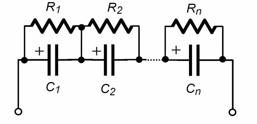
If the charging circuit has a voltage compliance that is set to the sum of the rated voltages of capacitors there is the risk that some of capacitors will be charged above the voltage limit. It is necessary to use some methods to prevent this fact. The simplest passive method for realizing a voltage balance is the circuit shown on Fig. 2. The balancing circuit uses for each capacitor C1 to Cn a resistor R1 to Rn, connected in parallel to it.
The values of resistances are chosen according to the supercapacitor leakage current. This parallel connection of resistors is widely used for series connected electrolytic capacitors. This resistive balancing circuit can balance the voltages in the stand-by regime and provides no dynamic balancing. Another drawback is the energy loss during charging-discharging process that limits the usage of the circuit in low-power applications or low charge/ discharge rates.

Another method for balancing the SM voltages is the circuit presented in Fig. 3. The circuit consists of Zener diodes DZ1 to DZn parallel connected to supercapacitors, instead of resistors. The maximum charging voltage of a capacitor is limited by the diode due to clamping voltage. This circuit has the advantage over the resistive one on the fact that there are no power losses before the capacitor has reached the rated voltage and also in the stand-by regime.

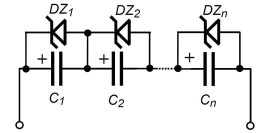
The main disadvantage of this kind of balancing circuit is the lack of dynamic voltage balancing capability. In fact, it would be possible to achieve dynamic limiting of the voltage, but it would require high power clamping diodes. The difficulties in implementing the circuit come from the use of low voltage Zener diodes (2.4-2.6V).
High current and high power Zener diodes are not available in this voltage range. Supplemental, the diodes breakdown voltage Vz is affected by large parameter dispersion and exhibit large temperature variations. A better circuit should perform automatic voltage balancing and prevent the over-voltage occurrence of individual supercapacitors in series connection while maintaining the charging current for the SM.
The solution for this balancing circuit presented in Fig. 4 is based on switched resistors. The circuit consists of resistors and switches SW1 to SWn. The
resistors R1 to Rn are connected in parallel with the capacitor C1 to Cn using the switches SW1 to SWn.

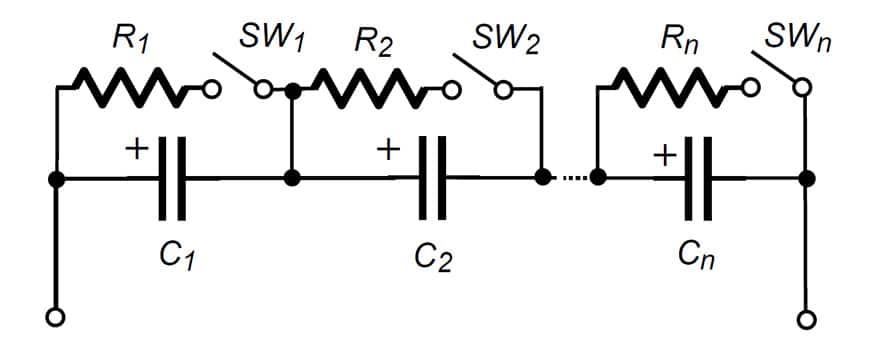
The capacitors’ voltages are monitored and if the voltage increases above a pre-established threshold (2.5V for instance) a command is given to the switch. This way, the charging current is diverted through the resistor. After the capacitor voltage has been naturally reduced (due to self discharge) to a value below the reference voltage, the switch will be turned off.
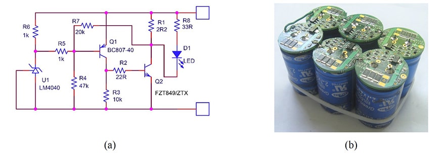
There are some power losses in resistors when the switch is on, but anyhow this circuit represents a good balancing solution. A solution to implement this circuit is to use transistors as bypass switches and voltage references for comparing the capacitor voltages with the chosen threshold. The schematic of a balancing circuit built using this principle is shown in Fig. 5 a) and a picture of the practical realization in Fig. 5 b). [3]

and balancing circuits attached
The circuit was designed for a voltage about 2.62 V and a bypass current of up to 1A. The limitation in current domain is determined by heat dissipation in R1 and Q2. The operation principle is based on diverting the charging current through a resistor (R1) and a transistor (Q2), as presented in previous section.
When the voltage at capacitor terminals reach the preset limit, the transistor Q1 begins to conduct the current through it and this leads to opening of transistor Q2. Transistor Q1 is a small power SMD transistor BC807-40 and Q2 is a high current, high power transistor FZT849. The resistor R7 provides a positive feedback that accelerates the on switching of transistor Q2.
The voltage reference is provided by the precision band-gap reference circuit LM4004 and was internally set to 2.048V. The LED is intended as an indicator and will be on when Q2 will be turned on, this means when the balancing circuit is active. A better solution is represented by the new developed intelligent circuits for supercapacitors charging and control. A solution based on principle shown in Fig. 4 is presented in the next section.
II. Intelligent Balancing Circuit Operation Mode
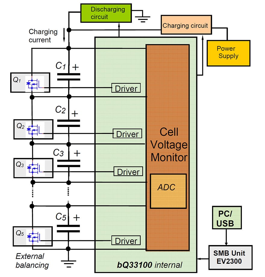
In our implementation of an intelligent balancing circuit we have used the integrated circuit bq33100 [1] which provides not only balancing of supercapacitor modules. It is in the same time a single-chip solution that provides many features for charge control, monitoring, and protection. It can individually monitor either 2, 3, 4, or 5 series of supercapacitors with individual balancing or up to 9 series capacitors with less control, only the stack voltage being measured. The bloc diagram of the system built around bq33100 is presented in Fig. 6.

We have used an evaluation board from Texas Instruments (TI), built around the circuit bq33100. The board is set to charge a series connection of five of supercapacitors. The system includes a communication SM Bus adapter for connecting with a PC via USB port and a power supply. A specific, but customizable free software package from TI was also used [4].
The detailed schematic of the system is presented in Fig. 7. This is based on design recommendations and applications note from [1]. The power supply voltage of the board must be high enough to ensure the charging voltage of the supercapacitors bank, (>n× 2.5V), n being the number of series connected supercapacitors in the bank, or to ensure the minimal power supply of the IC.
The right side of the circuit is responsible for charging. The voltage used for charging being set by the stabilizer Q1 and the circuit D2, type TL431, a precision reference voltage. The charging process is controlled by the pMOS transistor Q6. There exists the possibility to use four charging voltages by controlling the on-off state of transistors Q2 and Q3, their gates are connected to the controlling circuit. The four possible voltage levels are 10.5, 11.1, 11.8 and 12.4 Volts.
Usually during charging we have always used the maximum level, the other levels are being used by the bq33100 circuits for other purposes, for instance the learning process that was previously mentioned. The maximum charging current is set by the values of resistors R2 and R3 connected accordingly to reference circuit D1. In present implementation Imax=Vref/Req with Vref=2.5V a typical value for D1, and Req=10Ω/2=5Ω. It results the maximum charging current of 500mA.

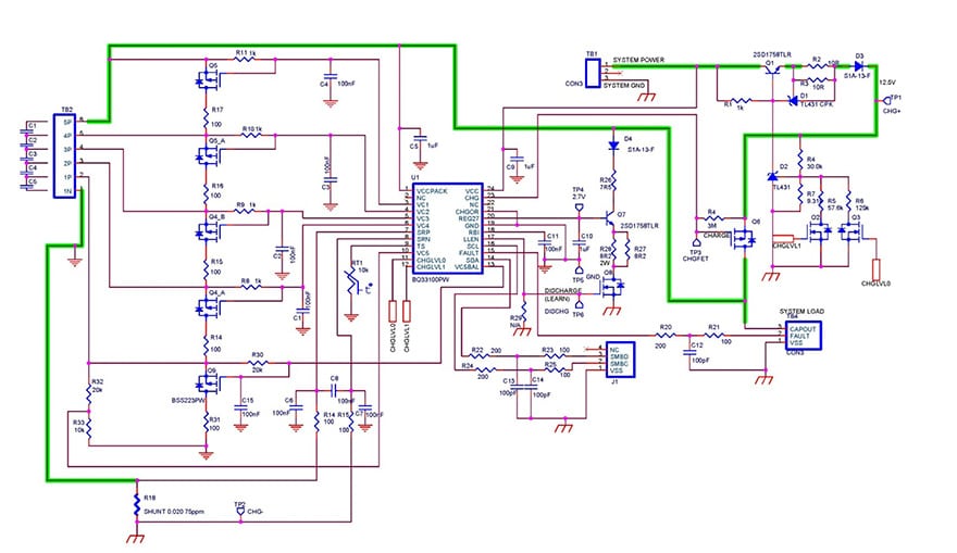
In the supercapacitor module the capacitors are connected in series and are attached externally at connector TB2. The common points between two adjacent capacitors are connected to the pins of IC bq3310, using the resistors R8-R11, with the required value of 1kΩ. The pins VC1-VC5 of the IC are used for voltage monitoring but also for balancing control. Exception here represents the terminals of the capacitor C5, for which there are provided two pins one for voltage monitoring (pin 10- VC5) and other pin (pin 13-VC5BAL) is used for commend of the balancing process.
The high accuracy in measurement is achieved by the IC using a 16 bit delta-sigma ADC with 16 channel multiplexing. The ADC is used for measuring all the individual capacitor or whole bank voltages and also for measuring the charge/discharge current and also for temperature measurement using the thermistor TH1. the current through the bank is measured using R18, a shunt resistor having 20mΩ.
The balancing is realized by driving the five pMOS transistors Q4 A and B, Q5 A and B and Q9. The load resistances are represented by R14-R17 and R31 having a value of 100Ω. This leads to a balancing current of 25mA, about the 20th part of the maximum charging current. Higher balancing currents are possible by lowering the resistance values. This eads to higher balancing speed on the expense of higher dissipation and more powerful MOS transistors.
Especially built for measurements of capacitance and ESR the board disposes of a discharge circuit built around Q7, Q8, R28, R27 R26 and D4. The bipolar junction transistor Q7 ensures the constant current, R27 and R28 are the sink load and Q8 is the switch for driving the discharging. Diode D4 is used for protection reasons. Without D4, when the voltage of the supercapacitor module is low, the pin REG27 of the IC is always at 2.7V and the base-collector junction of Q7 can be directly biased.
The integrated circuit bq33100 can be programmed to determine at certain time intervals or at specific command the capacitance and equivalent series resistance (ESR) of the supercapacitor module during normal operation. This process is called “Learning”. The main steps of this procedure, fully controlled by the IC, are presented in Fig. 8. The integrated circuit bq33100 performs the following sequence to determine Capacitance and ESR:
- Charge to V Learn Max, a value typically smaller than Vmax of supercapacitors, 2.4 V for a single cell, so 12 V for a 5 supercapacitor series module
- Discharge using constant current load (up to 500mA) to a certain voltage and record voltage and time
- Charge up to V Learn Max,
- Discharge using constant current load and internally record current and time
- Calculate Capacitance and ESR based on recorded voltage and current
- Determine new Charging Voltage for normal operation (5×2.4V )

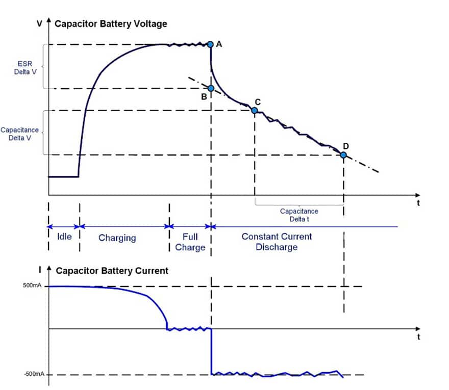
With the marked points in Fig. 8, we can use (4) and (5) to calculate the capacitance and ESR, respectively.


(4)
(5)
To ensure the serial communication a commercial available SMBus module EV2300 [5], from TI was used, connected at connector J1.

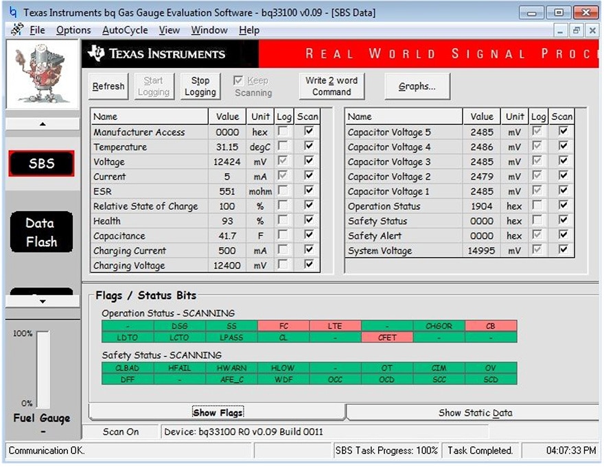
To communicate with the evaluation board we have used a free evaluation software from TI, called bqEVSW [4],[6] which has the possibility to change the registers of bq33100 and to set different parameters for operation. Most of default parameters do not need to be changed. We have changed the parameters especially for charging current and over-voltage, over-current protection.
The software of the IC uses advanced algorithms and the actual measured data to determine the SOC and available capacitance of the supercapacitor bank. A part of the working screen of bqEVSW is shown in Fig. 9. It can be seen the voltages at each capacitor, the almost finished balancing process and the flag registers FC- Full Charge, and CB- Capacitor Balancing being set (red color).
III. Results
We have tried the effectiveness of balancing for two capacitor banks, one uses 5 capacitors of 22F and the second bank having 5 series of 200F supercapacitors. The effective capacitance is 4.5F, respectively 40F. We have used a maximum charging voltage of 10.5V, that corresponds to 2.1V for a single capacitor. We have used different working scenarios.
One is that all capacitor begin charging process from the same SOC, and we monitor the individual capacitor evolution. The evolution of voltage starting from the same SOC, in this case zero, is presented in Fig. 10.

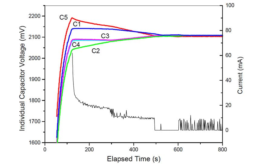
The circuit begins the balancing process just after the charge process is finished, that is the supercapacitor module voltage has reached the programmed value (10.5V) and the flag FC (Full Charge) is set. When the balancing process is started the flag CB is set. During this process a net current is pulsed through the bank, the peak value not exceeding 30mA, as can be seen in Fig. 7. It takes about 600s for a balancing of voltages in the range of ±1mV, which is fairy good. This includes the charging time of the supercapacitors stack.

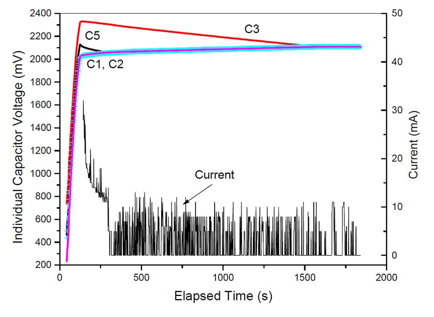
In a different scenario, the supercapacitor C3 (22F) was pre-charged at 700mV, the rest of supercapacitors being set at 200mV, so a difference of 500mV exists, a relatively large imbalance. In this case, the time needed to bring C3 to a voltage of about 2.1V was very long, of about 1600 seconds, as can be seen in Fig. 11.
A different situation, suppose that the charge process starts from voltages of 1.1V except the supercapacitor C2 that was charged at 300mV, so different from previous situation when a capacitor had a larger initial voltage. Now the difference in voltages is 800mV, a very large imbalance, that suggest a possible malfunction of the capacitor. In Fig. 12 are presented the charging curves.


It can be seen that in this case the time required to balance the voltages of all capacitors is very long, about 2800 seconds. In case of the 200F supercapacitor module the balancing was not possible in the limit of ±1mV, but ten times larger in the limit of ±10mV, obtainable after more than 1500 seconds starting from full charging state. We conclude that the only limit in using higher capacitances is the time needed for charging and balancing.
In Fig. 13 a) the measurement setup is presented showing the PC running the software bqEVSW, connected via USB to the EV2300 SMB module, the evaluation board and the supercpacitor banks on the left. Fig. 13b) presents a closer view of the bq33100 board.

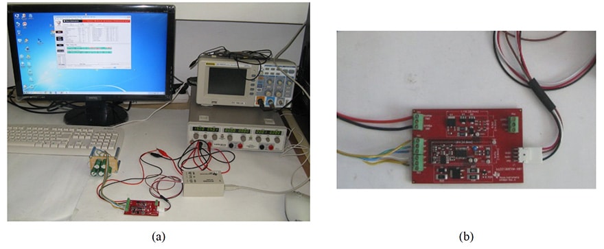
b) evaluation board based on bq33100 circuit
IV. Conclusions
Balancing of supercapacitor modules was performed using the intelligent circuit for monitoring and balancing. The evaluation circuit is performing well and in the limit of 600 seconds the balancing task for usual unbalancing voltages that can appear during operation. In case of larger differences at the start of balancing process, greater than ±100mV the process takes more than twice the mentioned time, depending on initial SOC.
The circuit needs to be modified for balancing a supercapacitor module including 200F capacitors, in the sense of increasing the charging current and the balancing current and a higher power capability for the sink load, R27/R28 in Fig. 7.
See also related in-depth technical article on supercapacitor balancing methods and its comparison.
References
[1] http://www.ti.com/lit/ds/symlink/bq33100.pdf, bq33100 datasheet, Texas Instruments, accessed March. 2019.
[2] P. J. Grbovic, Ultra-capacitors in Power Conversion Systems, John Wiley & Sons Ltd, 2014.
[3] C. Ionescu, A. Vasile, R. Negroiu, “Investigations on Balancing Circuits for Supercapacitor Modules”, 39th International Spring Seminar on Electronics Technology (ISSE) Location: Pilsen, Czech Republic,May 18-22, pp 521-526, 2016.
[4] http://www.ti.com/product/BQ33100/toolssoftware, Evaluation Software for bq33100, Texas Instruments, accessed Feb. 2019.
[5] http://www.ti.com/lit/ug/sluu159e/sluu159e.pdf, EV2300 Evaluation Module Interface Board User’s Guide, Texas Instruments, accessed Feb. 2019.
[6] C. Ionescu, A. Drumea, A. Vasile, N. Codreanu, “Investigations on Active Balancing Circuits for Supercapacitor Banks”, 41st International Spring Seminar on Electronics Technology (ISSE), Zlatibor, Serbia, May 16-20, 2018.
more 2nd PCNS symposium technical papers can be viewed and downloaded in pdf from EPCI Academy e-Proceedings: