
This paper High-Density PCB Assemblies For Space Applications: From Evaluation To Qualification was presented by Maarten Cauwe, imec and Ghent University, Belgium during the 5th Space Passive Component Days (SPCD), an International Symposium held from October 15th to 18th, 2024, at ESA/ESTEC in Noordwijk, the Netherlands. Published under permission from ESA SPCD organizers.
Introduction:
High-Density Interconnect (HDI) Printed Circuit Boards (PCBs) are pivotal in advancing space applications due to their capability to support modern integrated circuits like FPGAs, DSPs, and application processors.
HDI PCBs address demands for higher signal speeds, increased functionality, and compact designs, essential for space technology.
This paper, presented at ESA/ESTEC in the Netherlands, discusses the transition from evaluation to qualification of HDI PCB assemblies for space missions, highlighting the technological parameters, challenges, and reliability assessments involved in the process.
Key Points:
- Technological Drivers: Increased I/O counts, reduced component pitch, and high-speed signal requirements necessitate HDI PCBs.
- HDI Classifications: Differentiation between basic and complex HDI technologies based on component density and performance.
- Qualification Process: Includes stakeholder workshops, definition of technology parameters, and rigorous testing protocols.
- Reliability Assessments: Focus on microvia and core via reliability, interconnect stress testing (IST), and Conductive Anodic Filament (CAF) testing.
- Challenges: Balancing advanced manufacturing techniques with stringent reliability requirements for space applications.
Extended Summary:
HDI PCBs are essential for modern space applications that demand compact, high-performance electronics. These PCBs utilize microvias, high aspect ratio core vias, and fine line widths to support components with high I/O counts and reduced pitches. The initial phase of the project involved a stakeholder workshop to set requirements and distinguish between basic and complex HDI technologies.
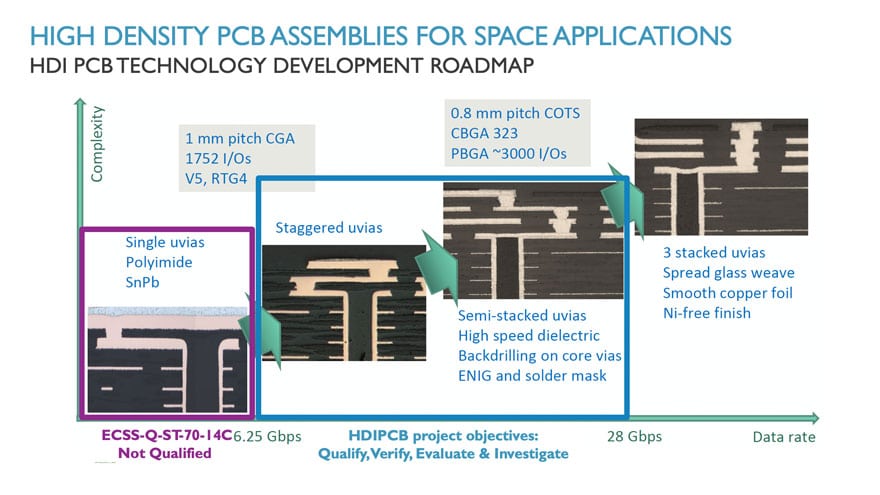
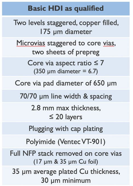
Basic HDI Technology targets immediate qualification goals with parameters tailored for large FPGA components and area array devices with 0.8 to 1.0 mm pitch. Polyimide remains the preferred material, supporting up to two levels of staggered, copper-filled microvias to ensure reliability without compromising on manufacturing risks.
Complex HDI Technology introduces advanced parameters like three levels of microvias, semi-stacked configurations, and high-speed materials for data rates up to 15 Gbps. The shift to polymer-based packages and finer pitches (0.5 mm) necessitates new reliability strategies, including solder mask requirements and alternative surface finishes like ENIG and ENEPIG.
The qualification process involved designing Qualification Test Vehicles (QTVs) to simulate real-world PCB designs, enabling comprehensive testing under ECSS standards. Initial qualifications faced challenges with microvia failures and core via cracks due to thermal stress. These issues highlighted the need for design revisions, such as increasing core via drill diameters and optimizing copper thickness for improved reliability.
Reliability assessments focused on interconnect stress testing (IST) and CAF testing to evaluate the endurance of microvias and core vias under thermal cycling and humidity conditions. The IST results underscored the importance of factors like copper plating thickness, aspect ratios, and the removal of non-functional pads to enhance core via performance. CAF testing revealed that contamination, rather than actual CAF growth, posed a greater risk to insulation integrity, emphasizing the need for meticulous cleanliness during manufacturing.
Further evaluations of the complex HDI technology showed promising results with some non-conformances related to dielectric cracks and solderability issues. These findings suggested that while the complex HDI technology is suitable for high-performance applications, its relevance for current space projects may be limited due to evolving component requirements.
Conclusion:
The study concludes that robust HDI PCB designs can meet the stringent reliability demands of space applications through careful material selection, optimized manufacturing processes, and rigorous qualification testing.
While basic HDI technology has been successfully qualified, complex HDI technology requires further refinements to address specific reliability concerns.
The continuous evolution of space electronics will drive future developments in HDI PCB technologies, ensuring enhanced performance and reliability for next-generation missions.
Read the full paper:

