
This article provides an overview of EMC requirements and the associated issues for the housing and the system. The post is based on Würth Elektronik‘s “Reference Guide ABC of Shielding” that can be ordered from WE website here. Published under permission by Würth Elektronik.
The overall system’s EMC performance must be evaluated in conjunction with housing attenuation, associated openings, and interface filtering, along with an associated ground system.
When considering radio interference emission, a portion of the interference is radiated through housing openings, while another portion is transmitted through cables.
As detailed in previous sections, a high shielding effectiveness of the housing necessitates a metallic structure with all-round contact, minimizing both the size and number of openings. Consequently, all sheet metal components should be seamlessly connected.
A high filter attenuation demands a low-noise, low-impedance ground reference system. This ground reference system can only be implemented if the shielding attenuation of the housing is maximized, and the interface filters are directly connected to the housing with the cable shields.
The key points are illustrated with examples below.
Gasket For Contact Between Connector Housing and Chassis
Even if there is no discrete (resistive) resistance in a circuit, there is always a certain resistance, which is increased by the skin effect due to the specific resistance of the conductor material. For example, a 5 cm long copper conductor with a diameter of 1 mm and a circular cross-section has a cross-sectional area of 0.785 mm2 and a DC resistance of about 1.0 mΩ at normal room temperatures. However, the resistance increases significantly at high frequencies, e.g., at 10 MHz the skin penetration depth is 20.69 µm, and the cross-sectional area associated with its first skin penetration depth is about 0.032 mm2, so its resistance is about 13 mΩ, which represents a 13 times greater heating effect (power loss) at 10 MHz than with direct current. At 200 MHz, the penetration depth is only 4.75 µm, and the cross-sectional area decreases to 0.00704 mm2, so that its resistance increases to 60 mΩ, which is 60 times higher than with direct current, and Thus, there is 60 times more power loss in the conductor.
Alternating currents flow as surface currents, and in shielding against electromagnetic fields, it must be ensured that all surface currents inside the enclosure remain inside and all surface currents outside the enclosure remain outside. The more surface currents that flow from the inside of the enclosure to the outside, the higher the emission of the fields emitted by the device. This applies not only to openings in the housing but also to connected peripheral cables. Shielded cables require 360° shielding over their entire length (i.e., no gaps) to prevent RF leakage. This applies to the shielding as well as the corresponding cable connector to the housing. Due to the skin effect, RF currents flow on the surface of the shielding, making it clear that a cable shield is a “tube-like extension” of the housing so that the surface currents inside the housing continue to flow within the cable shield. Any interruption of this current flow will inevitably lead to a reduction in shielding attenuation and, thus, an increase in interference emission. Figure 1. schematically shows the internal current flow in the interface area of an electronic device.
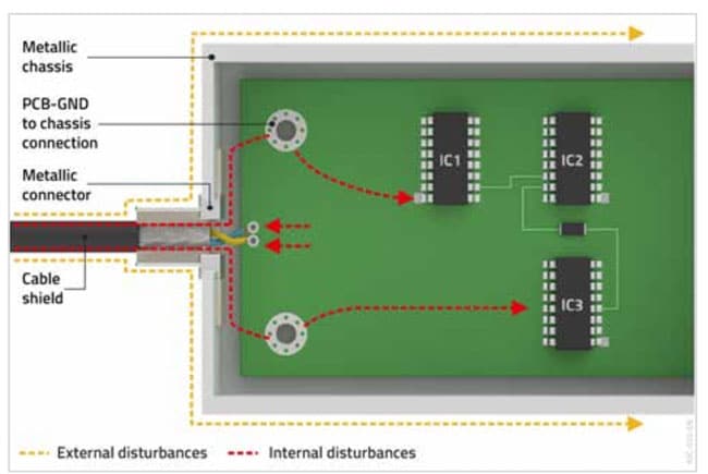
The electronics on the PCB in Figure 1. generate a useful differential mode signal, which is then fed into the signal conductors of the cable. The interface is symmetrical, with the signal flowing into one of the two signal wires and back into the other. Common mode interference currents flow to both signal wires and back through the red-marked path, passing through the board mounting, the inside of the metal connector, the inside of the housing, and the inside of the cable shield. The key point here is that these interference currents flow back due to the skin effect, on the inside surface of the housing and other components. Any interruption or discontinuity in this tube-shaped structure disrupts the “tightness” and potentially allows some interference currents to penetrate the housing and radiate as interference. The same applies if interference from outside affects the housing and the connected cable, as shown in orange in Figure 1.22. These interferences are coupled onto the surface of the housing and cable and must not be allowed to enter the interior. Any discontinuity in the housing or other components could weaken the shielding.
To enhance the shielding effectiveness of the cable shield and, if necessary, the interface filters, the system can be optimized, as shown in Figure 2. In this optimized system, the electronics board is not only connected to the housing via cable glands but also via the interface sockets. The interface sockets contact the housing wall via a conductive fabric seal, enabling a low-impedance connection between the interface filter, electronics board, interface socket, and cable shield. This connection is possible only if the interface plug has a metallic housing, which is typically the case with USB and Ethernet cables with shielded cable.
Figure 3. graphically illustrates the concept described in Figure 2.

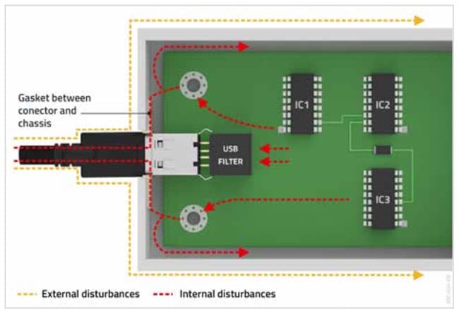
The direct RF-compatible connection between the filter, USB socket, and housing to the cable shield offers several advantages:
- Internal interference currents are minimized or eliminated, reducing the risk of cable damage.
- The USB filter receives a stable ground reference through the direct ground feed of the USB socket housing, enhancing its performance.
- Interference emission from the cable is significantly reduced, improving the overall signal quality.
- Cable interference immunity against fast transients and coupled fields is significantly enhanced, ensuring reliable communication.
- The interference immunity at the housing interface itself against ESD is significantly increased, protecting the housing from electrostatic discharge.
Fabric Seals and Spring Inserts For Housing Openings
In the previous sections, it was discussed that the shielding effectiveness of the housing and the shielded peripheral cables decreases with the size and number of openings or discontinuities within the housing. Additionally, electromagnetic interference can be radiated from the housing through gaps and openings.
Figure 4. illustrates how gaps caused by adjacent metal sheets in the housing can be prevented by applying additional seals or spring washers.

This measure increases:
- The shielding effectiveness of the entire housing
- The shielding effectiveness of the connected peripheral cables
- The immunity of the housing against ESD
Shield Design At The Board Level With Suitable Material Selection
The electromagnetic compatibility (EMC) behavior of a product is determined by the EMC behavior of its sub-components. For instance, if the electronic circuit board exhibits exceptionally low RF-emission, the shielding requirements for the housing can be reduced, thereby minimizing costs. The EMC behavior of the electronic circuit board can be significantly enhanced through appropriate design. For further insights into this topic, we recommend referring to the book titled “Trilogy of Magnetics” (ISBN 978-3-89929-157-5) and Passive components knowledge blog on inductors, which provides a comprehensive explanation of this subject.
However, for certain types of circuits, such as those in the field of HF power electronics, circuits with high reception sensitivity (radio receivers), high efficiency switching circuits (switching regulators), circuits with large signal bandwidth (audio technology), and circuits in the field of microwave technology (SAT range), as well as in special interference environments (automotive and industrial settings), reduction of interference emission and enhancement of RF-immunity may be limited.
In such cases, it becomes prudent to integrate additional partial local shielding and grounding at the PCB level to mitigate interference.
Interference Sources on The Circuit Board
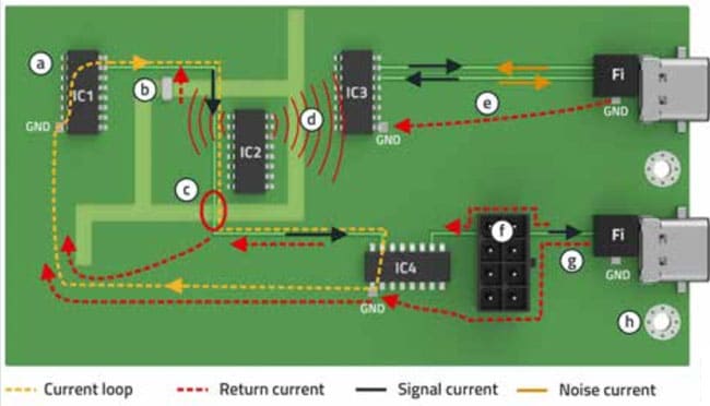
At this point, the principles of the origin of interference sources on the electronic circuit board will be briefly discussed. Figure 5. shows an overview of the possible interference source phenomena.
Explanation of the interference phenomenon:
IC1 generates a switching signal that travels to IC4 via a trace path. IC2 is placed in its own isolated area, with the GND layer below the signal layer and the power supply layer cut out. This creates an impedance change (c), which can be significantly reduced by a capacitor, known as a gap capacitor (b). The capacitance value depends on the signal, typically 1 nF at a signal bandwidth of 100 MHz. At point (c), the return current path is interrupted due to the impedance jump (high impedance), and the high-frequency return current takes the path of lowest impedance, shown in yellow. This results in a large signal current loop area, leading to high noise emissions.
Let’s assume IC2 generates a strong magnetic interference field (d) due to its internal IC structure and/or possibly also due to the ground conditions on the printed circuit board. This interference field is coupled into the adjacent conductor path (b) as well as into IC3, causing EMC interference and signal integrity problems. The emitted noise will also be noticeable as common-mode interference on the tracks of the balanced interface (e). The filter (Fi) may keep these tracks away from the interface port, but due to the large area of the current loop back to IC3, as shown in red dashed lines at (e), the filter current can lead to RF emission interference.
The effectiveness of the filter depends largely on the available ground. The filter reference ground must be free of any GND noise and must have the lowest possible impedance to the housing for effective filtering of the interface or the connected cable shields. A solid screw connection (h) can contribute to this.
IC4 generates a desired signal to the filtered interface (g). Since there’s a terminal strip between IC4 and the interface for a device-internal connector (f), e.g., with ribbon cable, whose pins are very close together, the GND and VCC layers must be cut out in this area. Additionally, the track connecting IC4 to the terminal strip must be carefully designed to minimize interference.
Leading between the connector pins must be narrower or routed around, which might not be feasible in this instance. Narrow routing will cause a signal mismatch, and the absence of a ground reference underneath the signal trace will cause the signal return current to split up, as illustrated in Figure 1.26 in the (g) and (f) areas.
All these described layout weaknesses generate electromagnetic interference and also result in reduced signal integrity, which can lead to immunity issues. Often, design engineers are aware of these problems; however, the fundamental conditions necessitate that these problems be consciously accepted, at least partially. Figure 6. presents potential remedial measures.

The layout, physical effects on components, and unfavorable positioning can cause electromagnetic interference (EMC) problems. However, these issues can be mitigated through design measures.
For instance, IC2’s magnetic field radiation can be almost completely reduced by an additional tinplate shield (a). An additional capacitor (b) provides a more uniform ground plane beneath the signal trace. IC3’s symmetrical lines can shield it, preventing coupling from the environment. Additionally, bonding a ferrite foil (e) over IC4 and the interfering lines significantly reduces radiation. The filter ground (d) can be substantially improved by conductive seals or contact springs between the sockets and the housing wall.
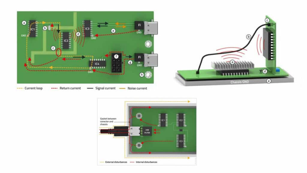
Figure 7. illustrates another example of electromagnetic coupling reduction. IC1 magnetically couples interference currents into the heat sink (a). Since the heat sink is electrically floating, these currents manifest as electromagnetic fields that couple into the cable (b). A similar phenomenon, without a heat sink, can be observed with IC2. The entire system is connected to the device chassis (e) via a screw (d). The circuit board of IC2 is electrically connected to the main board via the light blue connector (near (d)).
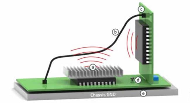
Figure 8. illustrates the potential measures to enhance electromagnetic compatibility. The heat sink IC1 is connected to GND via additional brackets (a), thereby serving as an additional shielding layer. However, when dealing with interference-intensive components, it’s crucial to ensure that the ground or GND potential remains unchanged due to the interference. Instead, the interference should be diverted through a low-impedance connection to the source of interference, which is IC ground.
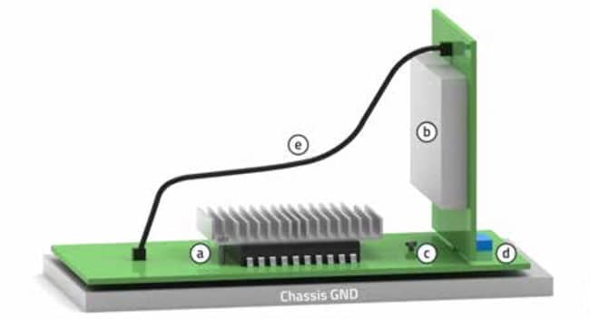
Equivalent to this is the shielding of IC2, where an additional tinplate shielding cabinet (b) is placed over the IC. Additionally, ensure that the GND surfaces of the electronic circuit boards are connected to the housing ground with low impedance using a plug connector (d) and a screw (c). The circuit board must, of course, have appropriate contact terminals available at these points. A further measure is to shield the cable (e), but the cable shield must be connected short at both ends to ensure it has low impedance to the GND surface, as only then can magnetic fields be shielded.
Related articles:
- Electromagnetic Housing Shielding and Its Effectiveness
- Parameters of Shielding Attenuation
- Influence of Shielding Materials on Shielding Effectiveness
- Electromagnetic Emissions Leakage in Enclosures

