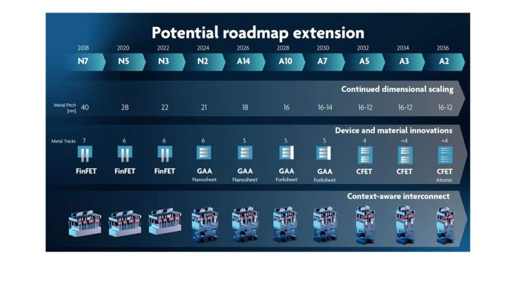
Belgian research lab IMEC has charted the roadmap path to semiconductor process technology and chip design below 1nm down to the A2 two angstrom generation.
At the recent Imec Technology Forum in San Francisco, Imec CEO Luc Van den hove laid out a 20 year roadmap for the evolution if semiconductor technology.
“We are convinced that Moore’s Law will not stop, but there will be many approaches that will all contribute,” said Luc van den Hove, CEO of IMEC
Future transistor architectures may include GAA devices built from a stack of nano sheets, den hove described several including a gate-all-around device built up of a stack of nanosheets and the forksheet device in which the N and the P channel transistors are moved closer together and the CFET where N and P transistors are stacked on top of each other.
“This forksheet device, we see as an extension of the standard nano sheet concept, and we believe it will be introduced around the equivalent of the one nanometer generation,” said Van den hove.
“It’s clear that you can realize another very important step in cell size shrinking, but obviously at the expense of much more complex contacting schemes to contact the source and drain areas. But we believe that we have developed integration schemes that would enable such transistors by optimizing the epi processes, patterning processes, and leveraging very sophisticated deposition processes to enable the contacting structures,” said Van den hove.
Possible ways ahead are reducing the thickness of the silicon channels to reduce channel length by replacing the silicon with 2D materials — atomically flat mono layers — such as tungsten or molybdenum sulfides or selenides.
“We’ve recently demonstrated the first versions of devices fabricated using 300 millimeter equipment,” he said.
But we also need to improve the performance of the interconnect. One interesting option is to move the power delivery to the back of the wafer. This leaves more design flexibility for the interconnect on the front side. “All of this results in scaling for the next fifteen to twenty years,” he said.
A combination of continued dimensional scaling, new transistor architectures, new materials introduction, combined with innovative interconnect architectures (buried power rails) will be the secret to success.
“We believe that we can propose a roadmap for the next eight to 10 generations — with an introductory pace of two to two-and-a-half year cadence — would bring us a roadmap for the next 20 years,” said Van den hove.
“We need to take into account the sustainability of manufacturing of these devices, the electricity use, the water, the chemicals. In optimising these processes it is not enough to look at the performance, power and area but we have to take into account the environmental aspects of these technologies.
