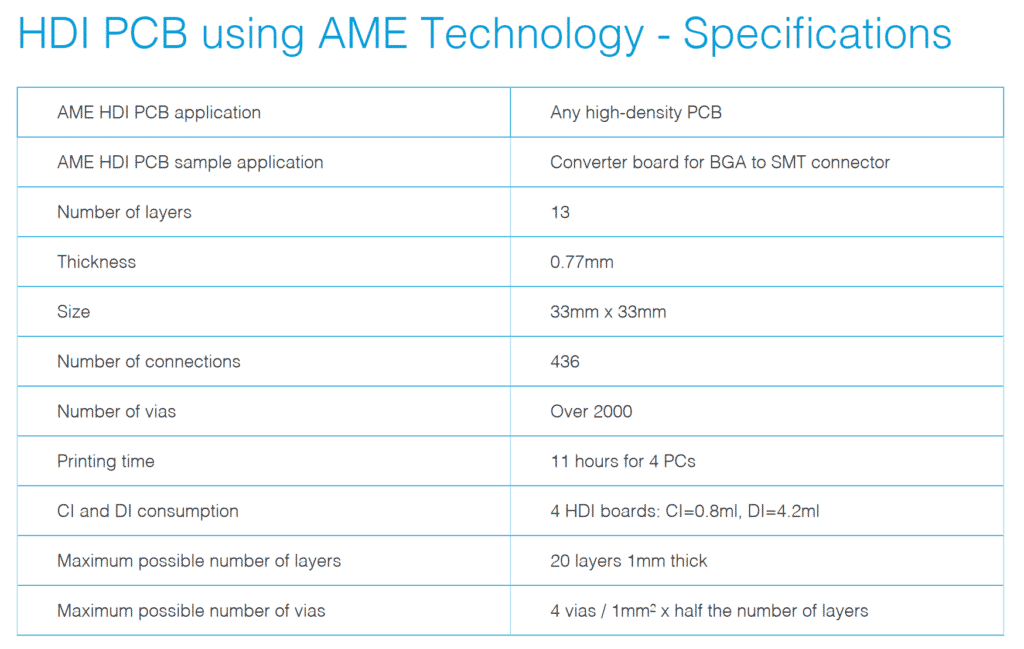
The ongoing technological revolution continues to introduce more and more innovative design and production methodologies for manufacturing highly- efficient electronic PCB products. One of this is High Density Interconnect (HDI) PCB by Additively Manufactured Electronics (AME) technology.
Being multi-layer, HDI boards have both buried and blind vias to provide more interconnections and signal integrity solutions. To achieve the desired stack up layers or sequential lamination cycles, conventional manufacturing processes require multiple drilling procedures that inevitably increase the time, complexity and cost of production.
Nano Dimension AME technology combines all bonding, lamination, drilling and plating into one simultaneous, short and comprehensive high-quality printing procedure. In fact, the lead-time for printing an HDI PCB using AME technology is about the same as for producing a standard plated through hole PCB.
Process Complexity and Duration
The conventional manufacturing of a plated through hole PCB is a multi-step process that requires lamination, drilling and plating. Manufacturing an HDI PCB requires laser drilling, plating and then adding top / bottom layers. This adds complexity and increases the duration of the process as the number of layers increases. An HDI PCB with 6 layers and stacked vias takes between 2 to 3 weeks to manufacture. With AME technology, printing a 60mm x 60mm x 1mm PCB board takes less than a day, regardless of the number of stacked vias and layers.With conventional PCB manufacturing, creating a stack via using a back drill increases the prepreg thickness, and therefore the overall PCB thickness. The thickness of the prepreg of an HDI PCB manufactured using AME can be any size above the minimum requirement.
This one-step process additively builds the HDI PCB layers including the conductive layers, prepreg, PTH, stacked vias, solder mask and solder pads.Any number of layers is applicable within the total board thickness requirements (3mm) considering the thickness of the conductive and prepreg layers.
Impedance Control
Using a laser drill and then plating stacked vias can cause disconnections. Filling laser drilled vias is complex and staggering vias generates impedance control challenges. During production, vias are stacked with offset. This results in problematic extensions and impedance imparity.
With AME technology manufacturing stacked blind / buried vias is simple, assuring impedance control without stubs or losses from via stubs.
