
A new type of material generates electrical current very efficiently from temperature differences. This allows sensors and small processors to supply themselves with energy wirelessly. The new material with a strong Seebeck effect could revolutionize thermal energy harvesting. The new material was formulated at the Institute of Solid State Physics at TU Wien.
Researchers have developed a new material that converts heat into electricity significantly better than previous thermoelectric materials. The discovery could be an enormous boon for the Internet of things.
Solutions based on batteries are becoming much more efficient and increasingly miniaturized. It is not possible to improve batteries enough for certain applications, however, such as sensors for the Internet of things, which aim to be zero-energy. These are devices that will instead rely on energy harvesting technology.
Energy harvesting refers to the ability to collect from the environment, or from the system itself, the energy necessary to power the electronics. Interest in energy harvesting has stimulated the development of complementary technologies, such as ultra-low-power (picowatts) microelectronics and supercapacitors.
This is where thermoelectric materials — materials that can convert heat into electricity — come in to play. This unprecedented capacity could be used to provide an autonomous and renewable energy source for a wide range of technologies, such as sensors or even small computer processors, enabling them to generate their own energy from temperature differences. The advent of increasingly efficient devices could pave the way for new solutions that take full advantage of energy harvesting.
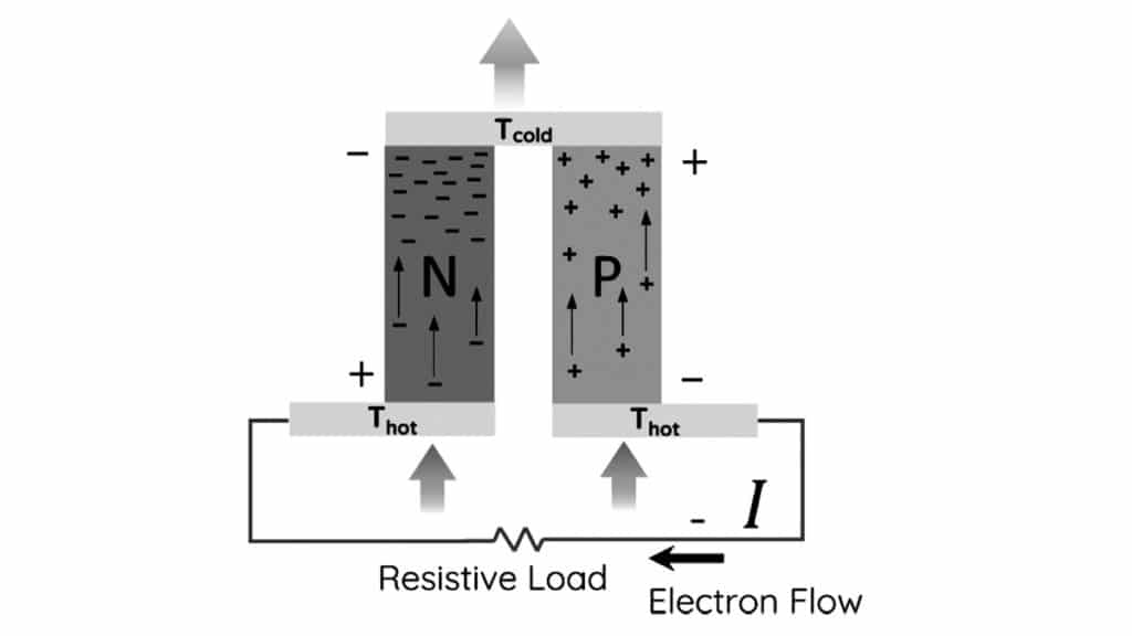
The Seebeck effect is when a temperature gradient between the two sides of a material generates an electrical voltage. The PN junction is the basic component of a thermoelectric device (TEG) and comprises a single structure of thermoelectric material types P and N realized by doping silicon with impurities such as boron (P) and phosphorus (N), each connected electrically in series.
featured image Figure 1: The TEG generator is essentially represented by a Peltier cell with two surfaces: hot (h) and cold (c)
A TEG module is essentially made up of many PN pairs placed in series. This structure generates a voltage proportional to the thermal gradient: the PN pairs are placed in parallel from a thermal point of view. The thermoelectric or TEG power generation modules are already used in many applications that collect the heat emitted by the decay of a supply of radioactive material (figure 1). The efficiency of this process depends on the temperature difference between the hot (Th) and cold (Tc) sides of the device and the performance of the thermoelectric material, expressed by the thermoelectric figure of merit ZT:

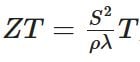
where S, ρ, and λ are respectively the Seebeck coefficient, the electrical resistivity, and the thermal conductivity, and T is the temperature at which the thermoelectric properties are measured. The so-called ZT value measures the amount of electrical energy that can be generated at a given temperature difference: the higher the ZT value of a material, the better its thermoelectric properties are. To improve the thermoelectric performance of a certain material, the power factor, PF = S2/ρ, must be increased and the thermal conductivity, λ = λe + λph, must be reduced (λe and λph indicate the electronic and phononic contributions respectively).
The efficiency of this thermal process is based on three parameters: the Seebeck coefficient, electrical resistivity, and thermal conductivity. These three individual physical properties that make up the figure of merit are not independent of each other. Therefore, improving one without deteriorating the other is difficult or impossible. λph(T) is the only quantity that can be changed freely without affecting the others. Therefore, the most promising way to improve overall efficiency is through size reduction. The study by Prof. Ernst Bauer from the Institute of Solid State Physics at TU Wien, focused on full-Heusler thin-film alloys deposited on Si wafers, due to their reasonably high PF and ZT values and their modest costs. In addition to the thermoelectric expectation, thin films can also be a basis for applications in fields such as microelectronics.
The best materials known to date have a ZT value of between 2.5 and 2.8. Scientists at TU Wien (Vienna) have succeeded in developing completely new material with a ZT value between 5 and 6. It is a thin layer of iron, vanadium, tungsten, and aluminum applied to a silicon crystal. The new, highly efficient material could revolutionize the sensor power supply market, especially in the Wireless Sensor Network (WSN) market. The use of battery-free solutions will make it possible to respect the environment. It is much smarter for sensors to be able to generate their own power from environmental sources. The new material was presented in the Nature Journal. The material thus produced has the advantage of being compact and extremely adaptable.
“A good thermoelectric material must show a strong Seebeck effect, and it has to meet two important requirements that are difficult to reconcile,” said Prof. Ernst Bauer from the Institute of Solid State Physics at TU Wien. “On the one hand, it should conduct electricity as well as possible; on the other hand, it should transport heat as poorly as possible. This is a challenge because electrical conductivity and thermal conductivity are usually closely related (figure 2).”
The new material has a regular crystal structure in the shape of a cube. The distance between two iron atoms is always the same, and the same applies to other types of atoms. The entire crystal is, therefore, completely regular. When a thin layer of iron is applied to the silicon substrate, the structure changes radically, and the atoms are assembled in an on space-centered structure with a completely random distribution. This distribution changes the electronic structure of the atoms and thus determines the path that the electronics take in the grids. The resulting electrical charge moves in a particular way, obtaining a very low resistance value. The portions of charge that cross the material are called Weyl Fermions. The irregularities of the crystalline structure inhibit the vibrations of the grids. The thermal conductivity is much lower, thus obtaining a good conversion of electricity from a thermal gradient.

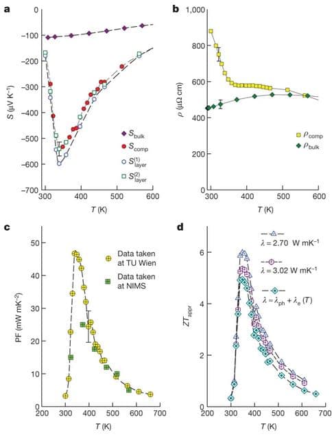
Measurements of electrical resistivity, thermal conductivity, and the Seebeck effect on the new material Fe2V0.8W0.2Al revealed very high values of the figure of merit for thin films deposited on a Si substrate. Experiments with electron microscopy also revealed a narrow diffusion zone between the Heusler thin film and the Si substrate.
Energy Harvesting offers significant advantages for the development and improvement of the Internet of Things. It is a key component in the creation of an advanced class of stand-alone and mobile applications that can run for extended periods of time without the need to recharge the batteries. By reducing the need for maintenance and battery replacement, Energy Harvesting enables intelligent sensing to be taken to remote or hard-to-reach locations within city infrastructure. This new study could also pave the way for new wearable solutions for the medical sector. With increased research and investment, the global market for the collection of thermal energy will reach a huge market, thanks to its ability to reduce costs and energy consumption.

