Source: Alter Technology article
Modern manufacturing techniques depend on 3D measurement data combined with CAD/CAM techniques for quality control of high-precision components or mass production. Typically, contact measurement has been widely utilized by the industry. However, for complex and small 3D structures, the application of contact measurement is cumbersome or sometimes impossible. Therefore, non-contact measurement has gradually received much attention from researchers and industry.

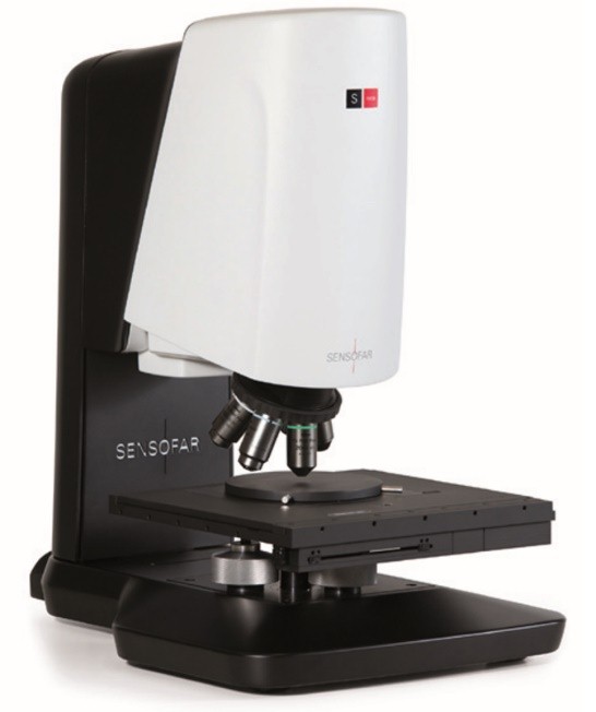
Confocal laser scanning microscopy (CLSM) is a non-contact optical imaging technique based on capturing multiple 2D images at different depths which enables the reconstruction of a 3D structure through a process known as optical sectioning.
The combination of the depth-discriminating ability of confocal microscopy and the digital image processing gives rise to fast and easy-to-use 3-D microscopy. Such technique can be used for material characterization, to extract statistical micro-geometric information, to evaluate surface roughness, to analyze the thickness of thin transparent coatings, and many other applications.
The information obtained by the CLSM process can be exported in different file formats, including 3D CAD files to be utilized in a third-party software (such as an electromagnetic simulation tool) or a 3D printer.
Enhanced Prototyping for Millimeter – Wave Waveguide Devices
Modern communications demand ever-larger capacity of the communication systems which have been progressively growing their requirements. As the low and medium range frequencies (up to Ka-band) have become saturated, industry and academia have focused in the exploration of the higher frequency bands for future commercial telecommunication programs. Therefore, the development of novel millimeter-wave devices is in the spotlight.
Waveguide filters are one of the key passive components embarked in the satellite payload or in-ground transmitters. As the frequency increases, the wavelengths become shorter and, consequently, the physical sizes of waveguide devices become smaller. This is an issue if conventional computer-numerical-controlled (CNC) milling is assumed as manufacturing technique, since the physical dimensions of the structure are of the same order of the fabrication tools. This produces unprecise fabrications, which urge the need of more accurate fabrication procedures such as high-precision CNC milling, deep reactive ion etching (DRIE) or UV lithography of SU-8. Although all the previous techniques are rather accurate, they all lead to systematic errors that should be considered in the design process to avoid frequency deviations.
CLSM can help to analyze the deviations of the selected manufacturing processes to speed-up prototyping activities. This is done by applying the errors detected in the part to perform a subsequent design of the wave guide filter. Once the CAD file obtained in the CLSM process is built, it can be simulated with an electromagnetic software (such as HFSS or CST MWS) to retrieve the measured frequency response. With this information, the designer could change the dimensions of the filter fulfilling the required frequency specifications to obtain a prototype whose measurements will be compliant.
At Alter Technology, we can perform 3D characterization using Confocal Laser Scanning Microscopy and the world’s most integrated and flexible test equipment for nondestructive 3D dimensional characterization, helping designers to get in-depth information about their prototypes.
Filters courtesy of Microwave Components Group – Public University of Navarre, developed under activity: “Waveguide filters fabricated by high-speed micromachining”.