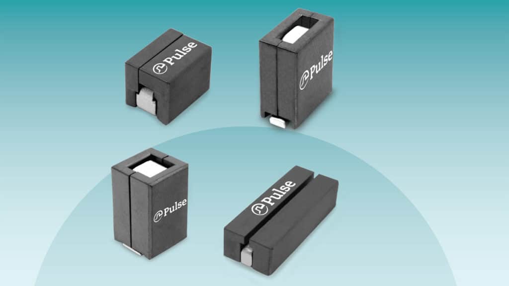
Pulse expands its range of power bead inductors with the introduction of six new platform sizes designed for the latest multi-phase and PoL architectures for server, graphics and high power FPGAs.
The latest platforms have ultra-low DCR, low loss ferrite cores and an optimized structure to ensure that they offer the highest efficiency and enable maximum power density.
The platforms range in size from 5.7×5.5mm to 10.8×8.2mm and come in inductances from 50nH to 1uH with peak current capability exceeding 120A and DCR as low as 120uOhms.
| Part Number Series | Footprint (mm Max) | Height (mm Max) | DCR (mOhms) | Inductance Range | Peak Current |
| PA4059 | 5.7 x 5.5 | 4.6 | 0.200 | 50-70nH | 50Apk |
| PA5041 | 7.2 x 6.7 | 11.2 | 0.290 | 120-330nH | 89Apk |
| PA4990 | 10.0 x 6.0 | 12.0 | 0.120 | 80-330nH | 178Apk |
| PG1712 | 9.6 x 6.4 | 9.3 | 0.170 | 150-300nH | 75Apk |
| PA4987 | 10.0 x 7.0 | 12.0 | 0.810 | 470-1000nH | 32Apk |
| PA5187 | 10.8 x 8.2 | 8.2 | 0.120 | 100-200nH | 100Apk |
“Pulse has long been a leader in power magnetics for computing and storage applications and these latest offerings add to the already significant portfolio of our high-volume, cost-optimized products. Our superior product, fast-turn prototyping and end-customer relationships enable us to maintain our leadership position”. John Gallagher | Product Marketing, Power PBU, Pulse Electronics
Although power beads can be used in a wide-range of applications, including input filters and single phase point of load (PoL) regulators, the most common implementation is as the energy storage element in a high-current multi-phase buck regulator. In these applications it is required to convert an input voltage (12v or 48v) down to relatively low output voltage (0.8 to 1.8v) but at currents that can change from 0A to 500Apk in a few hundred nanoseconds.
To protect the sensitive devices being powered these applications also require the output voltage to be very stable which necessitates minimizing the output ripple current. A single phase solution could be enabled but the ability to respond quickly (which requires a low apparent inductance) would be in direct opposition to the need for voltage stability (which requires a high apparent inductance).
By implementing a multi-phase topology, one avoids this conflict by breaking the current into multiple parallel paths. Each path has its own inductor and each path is activated (turned on/off) at different times throughout the cycle before being recombined at the output. This out-of-phase operation means that the ripple current in one path is increasing while in the other paths it is decreasing such that the ripple current partially cancels resulting in low output ripple.
The fact that there is ripple current cancelation at the output allows the inductance in each path to be significantly lower (50-250nH) and this in turn enables a much faster transient response.
These operational benefits of a multiphase circuit come at the expense of putting increased stress on the inductor. Although the output ripple current is drastically reduced, the ripple current in each phase, due to the low inductance, is very high.
If the inductor is not optimized the high ripple current will lead to excessive AC core loss and AC winding loss. In addition, the relatively low ratio of output voltage to input voltage (10%) means that the inductor effectively sees a much higher operating frequency which also contributes to high AC losses. Fortunately, Pulse is able to leverage our three-dimensional finite element analysis modelling skills, in depth material knowledge and vast design experience to ensure we optimize the design to minimize the AC and DC losses.
