
Source: IConnect 007 article
by David Hillman, Rockwell Collins.
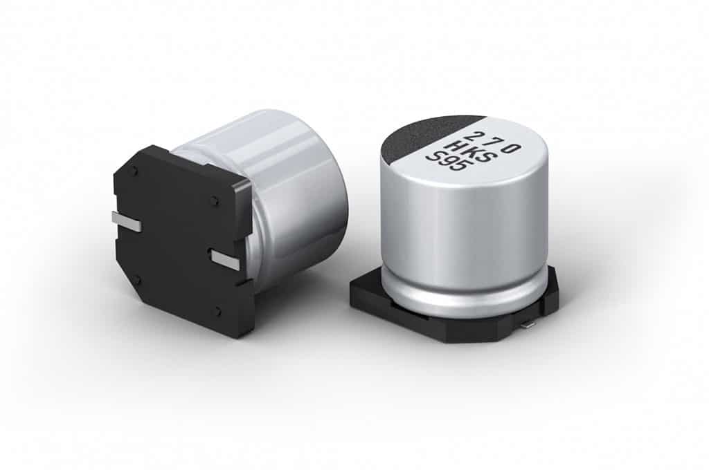
SMT electrolytic capacitors are a widely used component technology on IPC Class 3 avionics product designs. The body configuration of SMT electrolytic capacitors leads to solder joints that are only partially visible for optical inspection purposes. Figure 1 illustrates the obscured optical view of the capacitor lead due to the body construction/lead configuration. The capacitor lead exits from the bottom of the component and makes an “L” bend into the horizontal plane to provide surface area for the formation of a surface mount solder joint.
Featured Figure 1: Typical SMT electrolytic capacitor. (Photo Courtesy of Panasonic)

Figure 2: Solder joint workmanship criteria: gull wing (top), and lug lead (bottom) per the IPC-JSTD-001 Specification.
Significant debate/discussion of whether this lead configuration falls under a gull wing or a lug lead optical solder joint acceptance criteria (Figure 2) had transpired. Two key questions generated during internal discussions of this issue were:
- Does the existence of a solder joint heel fillet impact the solder joint integrity?
- Does the height of the solder joint side fillet impact the solder joint integrity?
The entire solder joint workmanship discussion would be a moot point if it were possible to print a sufficient volume of solder paste to ensure that both an acceptable solder joint heel and side fillets are created. That approach is not a viable option since this large amount of solder volume would lead to solder joint bridging and capacitor placement defects.
Concerns with SMT electrolytic capacitors were not limited to Rockwell Collins. The IPC-JSTD-001 National Standard committee formed a task group to investigate and create solder joint acceptance criteria for SMT electrolytic capacitors. The JSTD-001 task group consisted of avionics/commercial electronic assembly producers and component suppliers. The task group created a proposed set of solder joint workmanship criteria for SMT electrolytic capacitors (Figure 3). Rockwell Collins was in general agreement with the proposed workmanship criteria except for the Minimum Heel Fillet Height (G (solder thickness under component lead) + T (thickness of the component lead)), which the internal discussions had highlighted as a solder joint attribute that required further investigation. Note 3 in the table below is just the solder thickness under the component lead.
The SMT electrolytic capacitor is a standard component that has been widely used on various avionics products for several years. Therefore, any concerns about whether the capacitors were meeting the Rockwell Collins solder joint workmanship criteria after years of production was more a case of a new product auditor raising the question rather than a solder reflow process change. Two years of SMT electrolytic capacitor defect data was plotted to identify any type of process/product/people change influences (Figure 4). Since no changes in the reflow soldering process or the component configuration were documented, the defect variation illustrated in Figure 4 is the result of subjective, inconsistent solder joint workmanship criteria visual inspection (i.e. the solder height expressed as a percentage of the lead thickness (T) – a solder side fillet height 1/4T or 1/2T or 1T?). A review of product field failure data for the SMT electrolytic capacitor found no reported defects in 10,000 opportunities over an 8 year time period.

Figure 3: IPC JSTD 001 initial draft of proposed workmanship criteria for SMT electrolytic capacitors (Credit: Jim Dagget, Raytheon and IPC JSTD-001 SMT Electrolytic Capacitor Working Group).
In conjunction with the IPC-JSTD-001 working group effort to create solder joint acceptance criteria for SMT electrolytic capacitors. Rockwell Collins initiated an investigation to determine solder joint critical attributes using thermal cycle conditioning and shear testing. The test results would be used to create a recommended set of solder joint acceptance criteria for proposed inclusion in the Rockwell Collins Workmanship Standards and consideration by the IPC-JSTD-001 working group.
TECHNICAL DISCUSSION
Test Plan
A test plan was created with a focus on two solder joint attributes: (1) the mechanical strength of the solder joint; (2) the thermal cycle fatigue strength of the solder joint. One of the primary reasons for having solder joint geometry and wetting criteria is to ensure the creation of a consistent, repeatable solder joint that can withstand the standard mechanical stresses of a product use environment. While the primary purpose of solder attachment of components is to provide an electrical connection, some mechanical characteristics are expected. Due to their geometry, electrolytic capacitors traditionally require additional mechanical strengthening, with the use of adhesive bonding for vibration or shock purposes. The use of adhesive bonding practices allows for reductions in solder joint geometry and wetting requirements. Shear testing was included in the test plan to demonstrate that the board pad attachment failure would occur before solder joint failure. Solder joint thermal fatigue testing was included in the testing as it represents the primary failure mode of solder joints in avionics applications. The electrolytic capacitors would be subjected to -55°C to 125°C thermal cycle conditioning followed by metallographic cross-sectioning to determine the level of solder joint cracking resulting from the global Coefficient of Thermal Expansion (CTE) mismatch induced by the thermal cycling.

Figure 4: Process inspection solder defects for SMT electrolytic capacitors for a two year period.
Test Vehicle
The test vehicle used in the investigation was a typical printed circuit assembly that contained 10 of the SMT electrolytic capacitors, making it an excellent candidate for testing (Figure 5).
Test Component
The SMT aluminum electrolytic capacitor analyzed in the investigation was representative of SMT electrolytic capacitors used in the industry. Rockwell Collins procures these components from various industry component suppliers (Figure 6, Figure 7). The pad configuration is similar between the various suppliers, so the resulting solder joints are very similar. Since these components are susceptible to failure due to vibration in the product use environment, an enhanced pad configuration (Figure 7, Anti-vibration) is occasionally used with supplemental silicone adhesive bonding.


Figure 6: Typical SMT electrolytic capacitors. (Photo courtesy of Conrad Dubilier)

Figure 7: Typical SMT electrolytic capacitors. (Photo Courtesy of Panasonic).
Assembly

The test vehicles were assembled at the Rockwell Collins Coralville, IA production facility. The solder paste was Henkel MP-218 tin lead eutectic solder deposited with a 0.005 inch thick stencil. The components were placed using a Universal Advantis automated placement machine. The assemblies were reflowed in a Heller 1912EXL Reflow Oven. Assemblies were cleaned in the Electrovert Aquastorm 200 inline cleaner. The majority of the solder joint is obscured due to the package configuration, with only the outer end of the component lead being visible for optical inspection (Figure 8). The portions of the solder joints that were visually inspectable were considered non-compliant as they did not meet a 1T minimum side fillet height. The typical placement/spacing of the SMT electrolytic capacitors makes solder joint touch-up challenging and creates a potential opportunity for component or laminate damage.
Figure 8: Optical view of solder joints after automated reflow soldering.


Thermal Cycle Testing
The test vehicles were placed into a thermal chamber set for a temperature range of -55°C to 125°C. The ramp rate was set for 5°C–10°C per minute with 10-minute dwells at each temperature extreme. Figure 9 shows the thermal profile.
Figure 9: thermal profile of the test vehicle
After completing a total of 532 thermal cycles, the components were removed from the thermal cycle chamber for metallographic cross-sectional analysis.
Shear Testing
Prior to thermal cycle testing, a set of electrolytic capacitors were carefully removed from the assembled test vehicles for shear testing. This data set documented the typical as-soldered, not thermal cycled condition to provide a measurement of the strength of the solder joint wetting/geometry configuration. An Instron test system using a shear rate of 0.15 inches/minute was used for the test.


Figure 10 (left): test components/shear test setup
Figure 10 illustrates the test components/shear test setup. The measured mean peak load for the shear testing was 40.3 pounds with a standard deviation of 5.4 pounds (Figure 11). There are no industry acknowledged minimum shear force values, however, 30 pounds would be considered very adequate for solder joint integrity.
For comparison, the typical component pad peel strength is 6-12 pounds.
Figure 11 (right): peak load measurement table for the shear testing


Optical examination of the failed solder joints after shear testing revealed minor solder joint voiding, good wetting/solder joint geometry and complete metallurgical attachment for both the solder joint/component lead interface and the solder joint/component pad interface (i.e. cohesive failure).
Figure 12 (left): typical failed solder joint interfaces resulting from the shear testing.


Metallographic Analysis
A number of the SMT electrolytic capacitors were removed from the test vehicle after the completion of the thermal cycle conditioning for metallographic analysis. Some very minor cracking was observed in the solder joint heel fillet region but there were no observed anomalies in the solder joint microstructure or cracking that would indicate degradation of the solder joint integrity due to thermal cycle conditioning (Figure 13).
Figure 13 (above): solder joint metallographics analysis section
It was noted that a “1T” solder joint heel fillet or side fillet was not achieved using the standard automated reflow soldering process. The solder joint heel fillet height was found to be in the 1/2T height range.
Figure 14 through Figure 16 illustrate the solder fillet heights achieved with the standard automated reflow soldering process.

Figure 14: Cross sectional toe view of SMT electrolytic capacitor illustrating ~ 63% T side fillet height.

Figure 15: Cross sectional toe view of SMT electrolytic capacitor illustrating ~ 54% T side fillet height.

Figure 16: Cross sectional toe view of SMT electrolytic capacitor illustrating ~ 48% T side fillet height.
Discussion
The shear and thermal cycle test results clearly show that the SMT electrolytic capacitor solder joints have adequate solder joint mechanical and thermal fatigue properties. A 40-pound mean value validates that the solder joint is strong, and the metallographic assessment shows excellent wetting of all the solder joint interface regions.
The absence of solder joint cracking/failure after 500 thermal cycles demonstrates that the components meet a traditional avionics Electronic Components Management Program (ECMP) minimum requirement of 500 failure free thermal cycles. The metallographic cross-sectional analysis shows that the automated soldering process produces solder joint heel fillets and side joint fillets of approximately 1/2T. The practical limits of visual inspection are leading to inspectors misidentifying the fillet heights as 1/4T. A similar visual inspection problem was found for castellated solder joint fillet geometries on SMT filters [1].
Figure 17 and Figure 18 illustrate how visual inspection can be overly conservative in gauging the solder joint fillet height. The measured solder joint fillet height was 75% and not 50% per the visual audit. Inspection of the SMT electrolytic capacitors is a similar case of a “perceived” solder joint fillet height versus the “achieved” solder joint fillet height. The visual inspection of the solder joint height produced “false negative” response that lead to unnecessary rework of the components.
Since the automated reflow soldering process will always produce acceptable solder joint integrity, allowing a solder joint heel and side fillet height requirement of 1/4T would not be a concern. Similarly, manual soldering of the SMT electrolytic capacitors will always produce solder joint heel and side fillet heights exceeding 1/2T due to attributes of the process.

Figure 17: Castellation construction SMT component optical inspection vs. metallographic cross-section comparison. Audited optical inspection solder joint height under 50% fillet height [1].

Figure 18: Castellation construction SMT component optical inspection vs. metallographic cross-section comparison. Measured metallographic cross-sectional solder joint height measured equal to 75% fillet height [1].
Testing showed that a solder joint heel fillet and solder joint side fillet of 1T is not necessary to meet reliability requirements. A minimum requirement of 1/4T would be adequate for both the solder joint heel and side fillet height requirements for the standard soldering processes used for Rockwell Collins products.
Conclusion
The investigation of the SMT electrolytic capacitors was initiated to answer two primary questions:
- Does the existence of a solder joint heel fillet impact the solder joint integrity?
- Does the height of the solder joint side fillet impact the solder joint integrity?
The shear testing, thermal cycle testing and metallographic cross sections results demonstrated that the automated reflow process creates a solder joint with acceptable solder joint integrity. Deficiencies in visual optical inspection are resulting in a “false negative” assessment of the solder joint quality.
It is proposed that the industry Workmanship Standard criteria for SMT electrolytic capacitors be revised to the following criteria:
The minimum solder joint heel fillet and side joint fillet heights for SMT Electrolytic capacitors should be 1/4T.
Acknowledgements
The author would like to thank Coralville Common Process group, for test vehicle assembly and Richie Korneisel, Will Quandt, and Ben Theile, for metallographic cross-section processing, and Ross Wilcoxon for his scathing critique of the manuscript.
References
- D. Hillman et al, “Solder Joint Workmanship Criteria Investigation for Components with Castellated Solder Joint Configurations”, Rockwell Collins Working Paper, WP12-2001, 2012.
This article was originally published in the proceedings of SMTA International 2017.

