

This article based on Knowles Precision Devices blog explains role and function of switch filter banks in radar applications.
In the article RF Components for Radar Application, we provided an overview of the key functional units in radar, including duplexing, filtering, power amplification, waveform generation, low-noise amplification (LNA), receiving and analog-to-digital conversion (ADC). Here, we’ll focus on a particular form of filtering technology: switch filter banks.
Designing Agile Radio Frequency (RF) Receivers with Nimble RF Components
Today, modern radar systems are expected to serve in a multi-mission capacity. For example, the F-35 Joint Strike Fighter uses a multi-function array, where the radar active electronically scanned array (AESA) in the aircraft nose cone is shared between the electronic warfare (EW) and communications systems.
Tunable bandwidth is becoming more and more desirable. Designers need to be able to balance radar range and resolution and optimize performance across missions. Further, these systems need to operate reliably in a congested spectrum where there are many blockers.
In RF communications systems, unwanted input signals, otherwise known as blockers, directly or indirectly degrade the gain and signal-to-noise ratio (SNR) of the signal of interest. Blockers take the form of intentional and unintentional interference. Other RF communications systems operating in the adjacent frequency spectrum can cause unintentional interference, but so can malicious EW systems.
Agile RF receivers can be optimized moment-to-moment to adjust to evolving parameters. This level of control is accomplished using fully digital receivers with analog filter protection to evade blockers and prevent receiver damage. Nimble analog RF components, like switch filter banks, are critical to accomplish this level of optimization.
Switch filter banks are traditionally associated with larger footprints, but Knowles Precision Devices is leveraging materials science innovations to shrink the size of each individual filter. We use high-precision lithographic processes to pattern microstrip filters on our custom ceramics, and we develop low-loss, temperature-stable dielectrics that allow us to significantly reduce filter form factors (Figure 1).
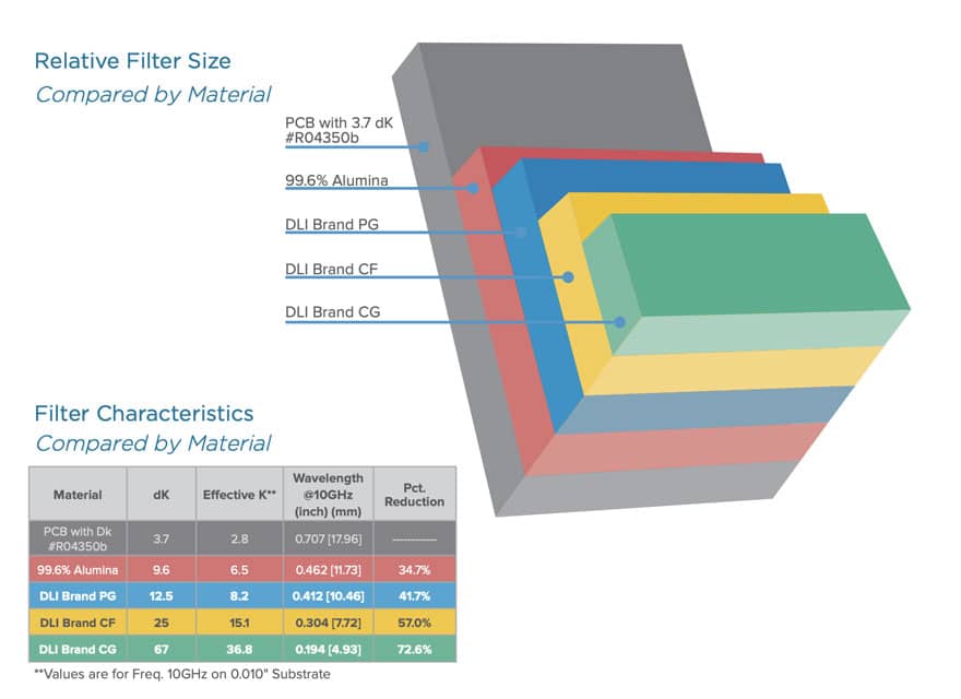
From there, our custom engineering team uses these miniature filters to create state-of-the-art multi-band filter structures that enable tiny switch filter banks.
Beyond miniaturizing filter components, there’s an opportunity to innovate around packaging. In partnership with Criteria Labs, we’ve established a small but reliable packaging concept for switch filter banks (Figure 2). With consideration for input size and how narrow the output needs to be, a designer has room for more channels.
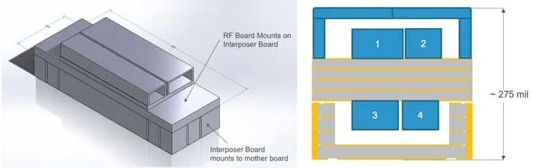
The design, based on a four-channel filter bank, features a 3D-stacked structure with alternating filters and interposer boards mounted directly to the printed circuit board (PCB). The result is a reduction in internal spacing that ultimately reduces the size of the filter bank.

