


GaN based RF devices offer significant advantages in a wide spectrum of applications ranging from commercial to high reliability / flight use equipment. This paper looks at the ability of Tantalum Polymer capacitors to be used on the voltage supply lines of GaN based Power Amplifiers. The fundamentals of Tantalum Polymers are presented along with recent products intended for flight systems.
A comparison of Tantalum Polymers to Aluminum Electrolytics & MLCCs in both electrical and environmental performance is provided. An example of a high power GaN RF transistor will be shown along side with performance features of each technology.
The paper was presented by Ron Demcko, AVX USA and Slavomir Pala, AVX Czech Republic at the 3rd PCNS 7-10th September 2021, Milano, Italy as paper No.4.3.
Introduction
Introduction
We are living in a world where increased electronic content controls, monitors and connects items commonly found in our daily lives. Examples range from our transportation systems to appliances, personal electronics to industrial process control systems. Regardless of the end item – electronics is everywhere.
Electronic proliferation into end devices is responsible for the high levels of performance that we all are very accustomed to and expect.
Additionally, careful implementation of electronics into end systems also provides efficiency gains and conservation of limited resources.
It is important to note that the control and communications circuits themselves are getting more efficient due to the low loss features of advanced semiconductor technologies. This makes it easier to utilize electronics in end devices since the electronics is smaller and requires less power to operate. In turn, electronic content in end systems accelerates further.
One of the most important recent semiconductor advancements to note is that of Gallium Nitride devices – GaN.
GaN devices show significant advantages over similar silicon devices in terms of efficiency, speed, operating frequency, power levels and temperature.
Equivalent sized GaN to Silicon die comparisons show massive current, voltage, power, and switching speed advantages, consistently favoring GaN. Alternatively, a GaN based semiconductor could be dramatically smaller than its Si counterpart if equivalent performance is the goal.
Regardless of the route taken – GaN has the potential to change both RF and power electronics design tremendously because of significantly reduced conduction losses (lower RDS-ON) and faster switching capacity due to reduced material capacitance and enhanced electron mobility. [1]
In short, use of GaN semiconductors may enable new applications to become possible – even practical or in less stringent applications make the circuit smaller, lighter & less power hungry.
For the purpose of this paper, we will concentrate on GaN semiconductors in RF power amplifier (PA) applications.
Three main areas considered where GaN technology improves the efficiency of the RF systems are:
- Reducing power supply distribution loss through higher voltage bias voltages thereby reducing current levels of similar power operation circuitry
- Reduced heat generation creates an opportunity for smaller thermal management solutions. That minimized need then results in smaller, lighter and potentially more reliable systems.
- Faster conduction /switching times
The GaN PA semiconductors in this paper are depletion mode devices that require a negative gate bias whenever there is a drain bias applied to prevent device damage.
Negative gate-source voltage must be present anytime the drain bias voltage is applied. [2] There are certain power up & power down sequences that must be followed in order to not damage GaN transistors. End users must insure those sequences always occur and many times utilize added hardware, software or a combination of both to achieve the correct conditions.
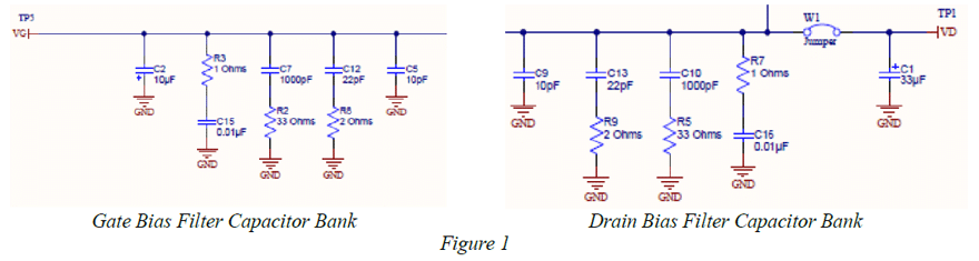
From a hardware point of view – banks of capacitors are used to filter noise in the bias lines and to provide charge during high di/dt demands of the amplifier during various operation conditions. The capacitor banks are chosen for stability over applied voltage & temperature as well as time/age of the device.
The frequency response of the capacitor bank is determined by both large value bulk capacitors as well as high frequency MLCCs (sometimes de-Q’d with series resistors). An example of capacitor banks used in GaN bias is shown in figure 1 below. [2]
The capacitors used in filtering these two bias lines play a critical role in PA operation are the area of concentration of this paper.

Filter Bank Capacitor options
Present day bulk capacitor options for the voltage bias banks range from high CV MLCC to Tantalum, Tantalum Polymer and Aluminium and Aluminium Polymer electrolytic capacitors.
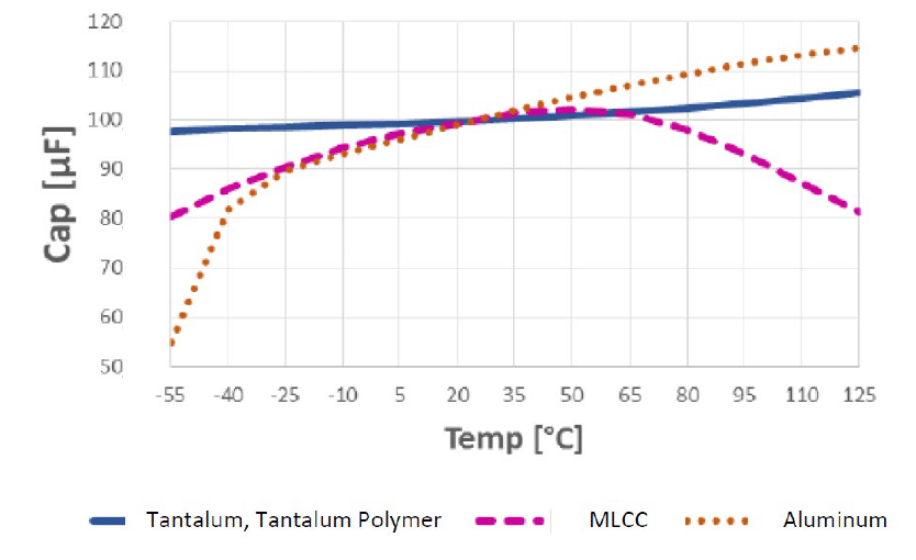
High CV MLCC capacitors can achieve the capacitance ranges used in many bias networks but do not provide the stability required for optimum GaN PA efficiency across operating conditions.
For example, capacitance stability of a 100uf X5R MLCC can vary from 100uf at 25°C to a capacitance of ~ 55uf at negative 55°C and 80uf at 125°C. In comparison, Tantalum, Tantalum Polymer, Aluminium and Aluminium Polymer electrolytic capacitors have adequate capacitance stability. (Near ideal stability in the case of Tantalum & Tantalum Polymer capacitors and acceptable stability in the case of Aluminium based devices). [3] Further, high CV MLCCs suffer from DC bias effects that can greatly reduce the capacitance value present in the actual circuit. This paper will not investigate high CV MLCCs any further for use as the bulk capacitor in bias networks due to the unstable capacitance associated with real world use cases.
The capacitance stability across common operating temperature range for all capacitor families discussed above are compared in figure 2.

Relatively low parasitic parameters (ESR and ESL) of bulk capacitors are advantageous to the response of the capacitor bank. One-step to reducing ESR of the bulk capacitor in the filter bank is to consider conductive polymer technology. However, the low ESL target eliminates wound aluminum electrolytic capacitors from further investigation in this paper. Though tantalum capacitors are used extensively in these bias applications – our attention will turn to polymer based capacitors where further reductions to already acceptable tantalum capacitor technology is possible from a ESR and ESL point of view.
Tantalum and Aluminum Polymer Capacitors
Tantalum Polymer Capacitors
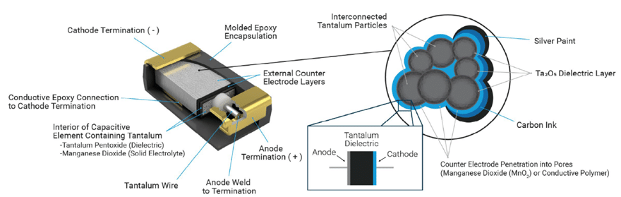
Tantalum Polymer capacitors are created by utilizing a conductive polymer in the cathode of the tantalum capacitor as shown in figure 3.
The anode wire is tantalum and a porous pellet of Tantalum powder is pressed onto the anode wire. The resulting structure is sintered into a monolithic block and a Ta2O5 dielectric is formed. A conductive polymer layer is deposited onto that structure and with added processing a tantalum conductive polymer capacitor is formed. This results in very low ESR devices compared to traditional Tantalum devices. ESR decreases of up to eight times are reasonable to expect and that translates into up to eight times the current capability compared to traditional tantalum capacitors.
Tantalum Polymer capacitors have added advantages of:
- Improved energy density allowing wide range of product values in smaller case sizes thus providing low inductance in face down/undertab designs
- Wide voltage range: 2.5v to 125v
- Lower de-rating required:
- 90% rated voltage / 10% voltage de-rating for products rated up to 10Vr
- 80% rated voltage / 20% voltage de-rating for products rated 16Vr and higher
- Benign failure mode if shorted
- No DC Bias voltage effects
- High Reliability – Space flight qualified & auto grade families available

A key feature of Tantalum conductive polymer capacitors is improved energy density and the flexibility that allows in providing reasonably sized capacitance ratings in small case sizes with reduced component height. Currently, case size dimensions can range from 0402 to 2924 and heights can be as low as 0.55mm.
Such small sizes translates into a capability of tantalum polymer bulk capacitors to withstand high levels of shock & vibration associated with automotive and flight applications.
Common conditions achieved are:

- Shock: MIL-STD-202, Method 213, Condition I, 100 G peak
- Vibration: MIL-STD-202, Method 204, Condition D, 10 Hz to 2,000 Hz, 20 G peak
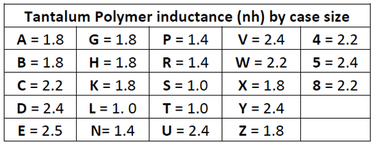
It is especially important to note that the broad range of conductive tantalum polymer capacitor package types and case sizes allow designers to place these capacitors at ideal PCB locations for maximum efficiency. Potentially smaller parts that have the capability to be placed in ways to reduce the loop inductance of the bulk capacitor relative to the capacitor bank. The wide number of different sized cases allows designers to utilize the ideal physical device in most applications. The inductance of Tantalum Polymer case sizes is shown in figure 4.
Aluminum Electrolytic Polymer capacitor
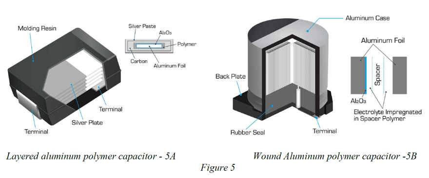
Aluminum Electrolytic Polymer capacitors come in either layered or wound styles. In the case of layered conductive polymer aluminum capacitors, a conductive polymer is the electrolyte. The layered devices have an aluminum cathode as shown in figure 5a. Layered aluminum polymers tend to offer reduced inductance over wound aluminum polymers – thus extended frequency response. Also layered aluminum polymers exhibit greatly reduced heights relative to wound aluminum polymers. Lowered height results in better shock and vibration performance as well as ease of implementation into height-constrained designs. The case of layered aluminum polymers is resin compound with J leads.
Wound conductive epoxy aluminum polymers are based upon a conductive polymer electrolyte but utilize a wound electrode structure vs stacked (as in the case of layered conductive polymers). Wound aluminum polymers shown in figure 5b) offer a larger capacitance range than layered aluminum polymers. In addition, wound aluminum polymers provide potentially lower ESR than stacked Aluminum polymer technology.

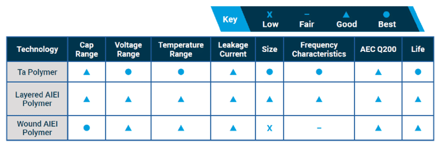
The prior device design explanations help understand the characteristics of these two devices in terms of Electrical and environmental performance. Figure 6 is a high-level comparison of the three technologies.

Tantalum Polymer Flight Approvals
The power, weight and volume advantages of GaN semiconductors is welcomed by the spectrum of flight platforms across the world.
Specifically, the ESA has published recognized advantages of GaNs as [4]:
- High output power density, small size, easy impedance match
- High voltage operation, simplified voltage conversion
- Operation under extreme environmental conditions
The desire to utilize GaN is understandable given that the cost to launch hardware can be considered approximately $25 per gram.
Tantalum Polymer Capacitors can complement and further GaN based system size & weight reduction.
Tantalum Polymer Capacitors be as small as 0402 case size with volumes as low as 0.363mm3 and weights low as 1mg. Such small size components are ideal for providing miniature bulk capacitance in advanced performance PAs.
Currently, NASA has Tantalum Polymer under review for flight use and the ESA has recognized Tantalum Polymer Capacitor technology for flight system use. ESA has approved TCS series capacitors in ESA 3012/006 as a Polymer MultiAnode Tantalum Capacitor Based on TCS Type. This family of parts has a maximum rated voltage of 50v. One very common used gate bias capacitor value is 10uf with a rated voltage of 35v. In fact, 35v rated ESA 3012/006 capacitor are approved in values up to 33uf, which may also potentially be used on low voltage drain bias filtering lines as well.
Hermetic encapsulated tantalum polymer capacitors are available as well in the TCH series – ESA3012/00*
The presence of excess moisture initiates a degradation of the polymer cathode material which is further accelerated by temperature and voltage (i.e. 85C/85% RV). The result is a loss in the polymer cathode conductivity causing an unpredictable drop in capacitance which is not generally recoverable. Though automotive AEC-Q200 and COTS-Plus grade Polymer capacitors are commonly used in moisture sensitive applications the hermetic packaged device offers even higher levels of enhanced performance.
Hermetic packaging of polymer capacitors was developed for extreme use applications in an attempt to suppress the impact of humidity and oxidization on the Tantalum Polymer capacitor. TCH capacitors are ideal for flight gate & drain bias banks with voltage ratings as high as 100v. Common values of use are: 22uf at 100v rating, 33uf at 75v rating, 47uf at 50v rating and 150uf at 35v rating.
GaN Application Example and Conclusions
GaN Transistor Example
A 125watt 50v DC-3.2GHz GaN transistor (Qorvo QPD1008) was chosen to use as an example where the use of tantalum polymer capacitors can reduce the size of existing 10uf tantalum capacitors used on the gate bias capacitor bank.
This design chosen is representative of a wide range of bias circuits but care should be taken to comply with IC house design recommendations since no blanket bias network can be used across all GaN transistors.
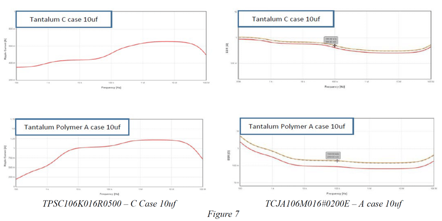
In this example the recommended gate voltage was -2.8v and the gate bias could range as low as -7v. The existing design called out a MnO2 based C case 10uf 16v rated capacitor (TPSC106K016R0500).
Changing to the tantalum polymer device reduces the case size from C case to A case. The area of a C case package outline is 19.2 mm2 vs. 5.1mm2. This change roughly yields a 73% reduction in board area. The A case capacitor (TCJA106M016#0200E) is also 1 mm thinner than the C case device.
From an electrical point of view the A case tantalum polymers smaller case size has 1.8nh of ESL vs. the C case having 2.2nh. This particular tantalum polymer reduces ESR by a factor of ~ 2 relative to the Tantalum device and its current capability is >2x that of the Tantalum capacitor.
Both ESR and RMS current comparisons between the existing tantalum capacitor used in bias designs compared to the smaller, lower ESR, higher current capable polymer are shown in figure 7. Comparisons such a these are accomplished through manufacturer simulation tools [5]. Lower ESR, smaller inductance and reduced case size make Tantalum Polymers a practical option for use in Vgs bias capacitor banks.

SUMMARY AND CONCLUSIONS
The use of GaN technology in RF PAs is virtually unstoppable due to significant advantages over Si technology.
Capacitor filter bank have a need for electrically stable low ESR/ESL bulk filter capacitors to insure reliable & high performance GaN device operation. Conductive Polymer capacitors are a possible alternate to existing solutions of Tantalum capacitors and Aluminium electrolytics. Most flight applications are concentrating on investigation and use of Tantalum Polymer capacitors on a minimum of gate bias line due to high energy density/small size. Consumer to commercial applications are also trending in this direction due to size and cost considerations.
REFERENCES
[1] Passive Components for GaN Based Devices; AVX Technical Notes 2021; https://www.avx.com/news/passive-components-for-gan-based-devices/
[2] GaN Bias Circuit Design Guidelines; Qorvo Technical Notes October 2019; www.qorvo.com
[3] Conductive Polymer Capacitor Basic Guidelines, AVX Technical Notes; www.avx.com
[4] ESA ESCCON 2013, GaN component technology development in Europe; www.esa.int/
[5] AVX SPITAN simultion software, https://www.avx.com/design-tools/tantalum-capacitor-models/

