
Source: TDK article
As part of its corporate mission of “Attracting Tomorrow,” TDK is dedicated to making advancements that break through existing technology limitations. One example presented in this article is the mass production of innovative, flexible sheet-type thin-film capacitors (TFCPs) that employ an innovative, new manufacturing method to overcome traditional thickness limitations of multilayer ceramic chip capacitors (MLCCs).
TDK’s TFCPs more effectively use the LSI package substrates themselves. These TFCPs help reduce the space typically required by the large number of decoupling MLCCs. Made of proprietary materials achieving a thickness of 50 μm or less, TDK’s TFCPs are embedded in the package substrate just below the LSI chip to deliver excellent decoupling effects at high frequencies.
These TFCPs are optimized for use as decoupling capacitors in high-end electronic devices such as data center servers, which require higher frequencies and higher speeds. Additionally, these thin-film capacitors are also ideal for use in wearables and various Internet of Things (IoT) devices, due to their thinness and flexibility.
Features of TFCPs from TDK
- Sheet-type capacitors comprising thin-film of dielectric material formed on nickel foil and superimposed with thin copper electrodes
- High dielectric constant achieved via dielectric material made of highly crystalline barium titanate (Relative permittivity: up to 1,000)
- Ultra-thin (thickness of 50 μm or less) and flexible to permit formation of vast variety of shapes
- Large number of capacitors embedded in the interposer of the build-up board
- Electrode pattern design flexibly delivering all desired capacitances
- Design contributes to making high-end electronic equipment (e.g., data center servers) work at higher frequencies, faster and with reduced power consumption
Major applications
- Built-in capacitors for circuit boards
- Decoupled high-speed LSI chips
Background
As a result of increased refinement in the manufacturing process of digital LSI chips such as semiconductors, microprocessors, memory and FPGAs, today’s LSI chips are faster and work at higher frequencies, and they are subsequently driving society’s advancements in information and communication technologies (ICTs). However, LSI chips are also prone to drive voltage reduction, necessitating a high quality of power or power integrity (PI) from power supply voltage. Voltage fluctuations in power lines may also destabilize the operability of electronic circuits, leading to malfunction and increased noise.
Manufacturers typically address these issues through decoupling or connecting a large number of capacitors between the power line and the ground (see Figure 1). In the event of a sudden change in the amount of current flowing to the LSI chip, voltage fluctuations are suppressed due to the electric load stored in the capacitor. Additionally, the AC component causing the noise is bypassed and sent to the ground. In other words, PI is improved by suppressing the impedance between the power line and the ground to a minimum, from the perspective of the LSI chip.


The ease with which AC passes through the capacitor is generally determined by both the AC frequency and the capacitance rate of the capacitor. As the frequency becomes higher and as the capacitance increases, AC passes more easily through the capacitor. Capacitors with inductance components and resistance components in the lead wires and electrodes that are not shown in circuit diagrams are known as equivalent series inductance (ESL) and equivalent series resistance (ESR).
Normally during decoupling, multiple capacitors are combined and connected in parallel, to attenuate the AC component over a wide frequency range. High-capacity capacitors such as electrolytic capacitors are used to bypass the AC component at low frequencies. At high frequencies, capacitors with low ESL and ESR are required to lower the impedance. MLCCs are widely used for decoupling at high frequencies because of their low ESL and ESR properties and excellent impedance-frequency characteristics.
The number of MLCCs installed around the LSI for decoupling may range up to 100. As LSI packages become smaller and thinner, it becomes increasingly difficult to ensure sufficient space for mounting the MLCCs. In general, decoupling capacitors are connected to the ground as close as possible to the LSI power supply terminal. This is done because when the wiring path is branched or is extended, the ESL and ESR of the wiring may cause the impedance to become high, thereby reducing the desired decoupling effect.
One effective solution is to use the inside of the circuit board to mount the LSI chip. Traditionally, engineers have created a cavity inside the circuit board for the purpose of embedding thin MLCCs. However, this popular method has limitations because of the thickness of the MLCCs manufactured using the multilayering process. The typical MLCCs thickness of approximately 0.1 mm makes it difficult to embed a large number into a circuit board. In contrast, TDK’s TFCPs have a thickness of 50 μm or less. As shown in Figure 2, these capacitor sheets can be embedded in the circuit board just below the LSI chip with a minimal gap, or embedded just below the bare chip inside the circuit board, as an alternative to arranging MLCCs around the LSI chip.


Figure 2 Built-in circuit board solutions from surface mounted MLCCs to sheet type thin-film capacitors (TFCP)
Optimizing Thin-Film Capacitors (TFCPs) with TDK’s Materials and Thin-film Technologies for use as Built-in Capacitors in Circuit Boards
TFCPs from TDK have a structure where a thin dielectric film is sandwiched between two thin metals (see Figure 3). During the manufacturing process, nickel foil with a high degree of purity is used to form the bottom electrode; a thin dielectric film made of barium titanate formed by a proprietary sputtering method forms the middle; and the copper top electrode is superimposed by thin-film formation.


Figure 3 Structure of the thin-film capacitor (TFCP) from TDK
| Major specifications/electrical characteristics | |
|---|---|
| Sheet thickness | 50μm or less |
| Capacitance | 1.0μF/cm2 |
| Relative permittivity | up to 1000 |
| tanδ | 0.1 or less |
| Operating voltage | 4V or less |
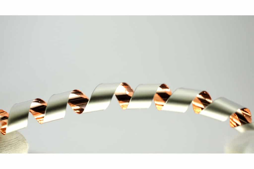
TDK has built custom production equipment for superior sputtering to form high quality dielectric film that is free of pinholes or cracks. This contributes to the achievement of extremely high yields during mass production. These capacitor sheets feature ultra-thinness (total thickness is 50μm or less) and flexibility, as well as resistance to damage even when wound around a rod as slim as a pencil.
TDK’s proprietary materials and manufacturing method have produced groundbreaking achievements in high capacitance (e.g., 1μF per cm2), in optimization of material design for the dielectric material made of barium titanate, in annealing (heat treatment) after sputtering, and in high crystallization of the dielectric thin-film, as well as achieved relative permittivity up to 1,000, which is an order of magnitude higher than previously achieved levels.
This article presents a method for sheet layering on a package substrate, mainly for LSI decoupling.
Embedding Large Numbers of Capacitors in the Interposer Board
Packaging and mounting technologies play significant roles in the high integration of semiconductor devices. The semiconductor package protects the chips from the external environment and also plays an important role in electrically connecting the chips to the PCB . An interposer that uses a build-up board in an LSI chip, such as the flip chip-ball grid array (FC-BGA) circuit board, is used as an intermediary package between the LSI chip and PCB.
The build-up board is manufactured using a process with lasers to form a via, or opening, in the top and bottom layers of the laminated board or the core layer. The layers are stacked, one by one, by electrically connecting the interlayers using plating. (Note, there is also a coreless thin type.)
An interposer in a build-up board is generally one to two millimeters thick. Because interlayers are each only 100μm, focus has shifted in recent years towards more effective utilization of the inside of the interposer board. Originally used in a package substrate, the build-up board was manufactured with extremely high precision when compared to PCBs.
The thin-film capacitor sheet pictured in Figure 2 shows the external appearance of the product before it has been turned into an embedded capacitor. As part of the embedding process, multiple sheets are layered on the circuit board during the interposer manufacturing process, and then converted to a large number of built-in capacitors. This occurs through the process shown in Figure 4 below.


Figure 4 Example of the process of embedding a thin-film capacitor (TFCP) in an interposer board
During the process, the TFCP sheet is cut to a specified size and shape. Next, the nickel layer that is the bottom electrode is patterned using photolithography. Additionally, the TFCP it is layered onto the circuit board with an insulation layer in between. Finally, the copper layer or top electrode is patterned.
A normal build-up manufacturing method follows. A laser is used to create a via in the insulation layer, and plating is used to electrically connect the interlayer, after which the wiring pattern is formed by photolithography. Patterning uses both the subtractive method to remove unnecessary patterns from the copper foil, and the additive method to add copper patterns on top of the insulation layer. By repeating this process, a 3D wiring path is built with a large number of capacitors embedded inside the circuit board.
As shown in Figure 5, thin-film capacitors are formed between the power supply plane and the ground plane just below the LSI chip. The greatest advantage of this design is that capacitance can be freely designed by electrode patterning, and a large number of capacitors can be embedded together. This novel method of embedding a thin-film capacitor with a unique sheet structure, using the build-up method, delivers a minimum gap from the LSI chip inside the interposer board just below the LSI chip. As such, the process achieves extremely effective decoupling, and also yields significant space savings on the package substrate.


Figure 5 Structure of an interposer board and pattern diagram of the built-in thin-film capacitor (TFCP)
Reducing Impedance by 73% Through Decoupling of Embedded Capacitors on the Circuit Board Just Below the LSI Chip
Figure 6 shows an example of simulation of the decoupling effect by building thin-film capacitors into a circuit board.
The graph depicts the simulation of the electrical characteristics when ① MLCCs are surface mounted on the reverse of the package, ② MLCCs are embedded in the circuit board, and ③ TFCPs are embedded in the circuit board and MLCCs are surface mounted.
In case of ① where MLCCs are surface mounted, a large impedance peak is observed at high frequencies in the 100MHz band. In the case of ② where MLCCs are embedded in the circuit board, the impedance peak at high frequencies is suppressed by about 50%, which is insufficient. In contrast, the example ③ is a package structure with built-in TFCPs where impedance is suppressed at high frequencies down to 27%. This is achievable due to the arrangement of thin-film capacitors just below the LSI chip to reduce the connection distance between the power line and ground line, thus achieving low ESL values that were previously impossible, and obtaining a significant decoupling effect.


Figure 6 Example of simulation of the electrical characteristics of various package structures
Summary
TDK’s TFCPs are unique sheet-shaped capacitors developed from the company’s extensive knowledge of materials, core technology, and thin-film technology, cultivated through decades of experience manufacturing HDD heads.
TDK started mass production of thin-film capacitors in 2016, and has begun supplying them for decoupling the CPU in high-end machines such as data center servers. Placing a TFCP inside the package substrate just below the LSI chip results in significant miniaturization and space savings as well as higher speed, higher frequency and reduced power consumption. These highly sought after attributes are expected to make a significant contribution towards managing the massive increase of information in the IoT.
The sheet structure also allows for capacitance to be increased with multilayering. Today, TDK is mass producing products with double the industry average capacitance. The company is dedicated to continuing its research and development with the goal of achieving a tenfold increase in capacitance in the future, and is working towards the development of new dielectric materials and sheets with robust features by making additional advancements in thin-film formation technologies.

