
This Analogue Devices article written by Jellenie Rodriguez and Mary McCarthy discusses thermistor-based temperature sensing system optimization and evaluation.
Introduction
As discussed in article Thermistor-Based Temperature Sensing System Explained, there are different challenges involved in designing and optimizing thermistor-based application solutions. These are sensor selection and circuit configuration, which were discussed in the previous article. Additional challenges are measurement optimization, which includes the ADC configuration and selecting the external components while ensuring that the ADC is operating within specification, and the system optimization to achieve the target performance and determine the error sources associated with the ADC and the overall system.
Thermistor System Optimization
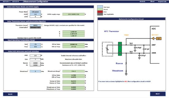
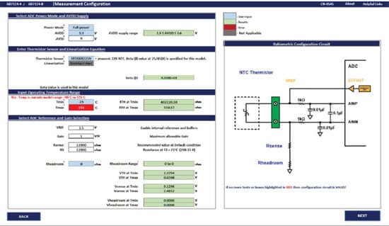
With an easy to use tool such as the Thermistor Configurator and Error Budget Calculator, customers can easily configure the thermistor in their system, including the wiring and connection diagram. The tool designs the thermistor system with an excitation voltage in a ratiometric configuration. It also allows customers to adjust the settings such as the sensor type, temperature range being measured, linearization, and external components as shown in Figure 1. It ensures that both the ADC and thermistor sensor are used within specification. So, if a customer selects an option that is not supported, the tool flags that this is an error condition. For example, if a customer selects a maximum temperature value that is outside the operating range of a specific thermistor model, an error will be displayed as shown in Figure 2. Following the recommended range value will again ensure that the system configuration meets the sensor and electronic operating conditions.
The tool enables the user to understand the different error sources, and it also allows design optimization. Note that the tool is designed around the AD7124-4/AD7124-8, so it also determines the number of sensors that can be connected to a single ADC. To appreciate the importance of the tool, let’s walk through the different design considerations used in thermistors.
System Configuration (Excitation, Gain, and External Components)
Similar to RTDs, thermistors are also susceptible to self-heating as resistors dissipate power when a current flows through them. Thus, the designer must keep the operating current of the thermistor as low as possible so that its power dissipation will not have a significant effect on the measurement results. Primarily, designers tend to select higher values of excitation voltage to generate higher output voltages so that it can make full use of the ADC’s input range. However, since the thermistor sensor has a negative temperature coefficient, its resistance decreases as the temperature increases, so a high value of current flowing through it will result in a higher power consumption that leads to self-heating.
On the brighter side, a thermistor does not require higher excitation source values as its higher sensitivity characteristics can generate an output voltage from millivolts to volts over the specified temperature range. Therefore, using an excitation voltage such as the ADC reference voltage value is sufficient, and it allows a ratiometric configuration. By setting the PGA gain to 1, this technique also ensures that the entire thermistor output voltage range or the voltage that is seen on the analog input of the ADC will always be within the ADC operating input range. The tool uses the internal 2.5 V reference available on the AD7124-4/AD7124-8. When a gain of 1 is used, the PGA is also powered down, reducing the overall current consumption. The AD7124-4/AD7124-8 also incorporate analog input buffers that allow unlimited resistance and/or capacitance values to be used externally, making them ideal for direct connection to external resistive type sensors such as thermistors or connecting electromagnetic capability (EMC) filtering without adding any error. However, when using the ADC at a gain of 1 with analog input buffers enabled, it is necessary to ensure that the headroom required for the correct operation is met. The tool also allows designers to balance the selection of external components including the allowable range for external headroom resistor and the recommended sense resistor value along with its tolerances and drift performance. The thermistor tool also provides a list of commonly used thermistor types and allows options where the designer can enter the nominal value and beta (β) or Steinhart-Hart constants of any type of NTC thermistor. The accuracy of the sensor, external components, and its contributions to the system error along with the effect of linearization technique used by the sensor will be discussed later.
Filtering and Power Consideration
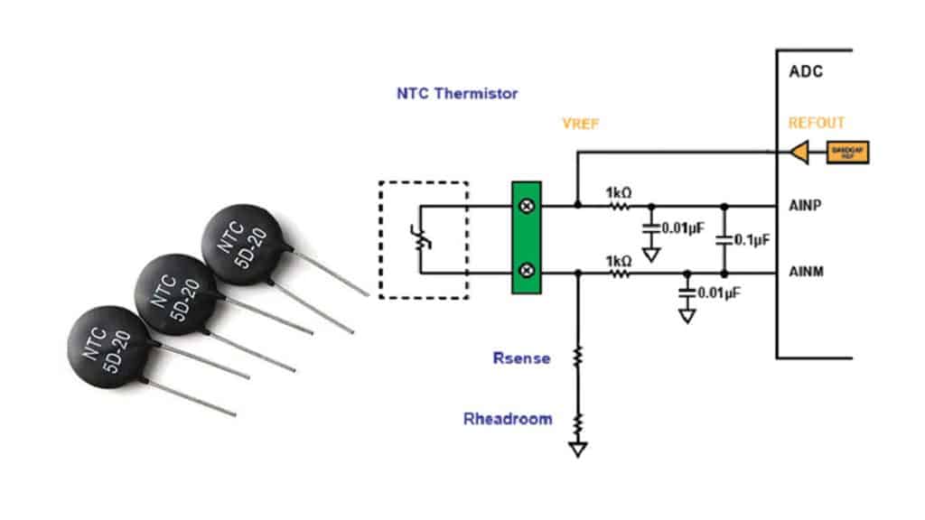
Sigma-delta ADCs use a digital filter, and the frequency response of the digital filter provides 0 dB of attenuation at the sampling frequency and multiples of the sampling frequency. This means that the filter response is reflected around the sampling frequencies so an antialiasing filter in the analog domain is required. Since sigma-delta ADCs inherently oversample the analog input signal, the design of the antialiasing filter is simplified such that a simple (single pole) RC filter is sufficient. For example, the AD7124-4/AD7124-8 will only require a 1 kΩ resistor in series with each analog input, a 0.1 μF capacitor from AINP to AINM, and a 0.01 μF from each analog input pin to AVSS.
In most industrial applications or process control, extra robustness is one of the top priorities. A system may experience noise, transients, or other interference from its neighboring components or environment. For EMC purposes, large R and C values on the analog input are typically used. However, please take note that when the converter is operated in an unbuffered mode with a gain of 1, the inputs look directly into the sampling capacitor of the modulator so large RC values can cause gain errors as the ADC does not have sufficient time to settle between sampling instants. Buffering the analog inputs prevents these errors.
Interference from the mains power supply can also affect measurement results. Thus, 50 Hz/60 Hz rejection is also one of the system requirements when devices are powered from the mains supply. Another benefit of a narrow bandwidth sigma-delta ADC such as the AD7124-4/AD7124-8 is it offers flexible digital filtering options that can set notches at 50 Hz and/or 60 Hz.
The selected filter type along with the programmed output data rate influences the settling time and its noise performance. The device also offers different power modes that allow the user to tune the ADC for optimum power, speed, or performance. The current consumption or power budget allocation of the system is highly dependent on the end application. If the system requires higher output data rates and better noise performance, then the device can be configured in full power mode. If limited power consumption is required at reasonable speeds and with reasonable performance, then the device can be operated in mid or low power mode.
Aside from the accuracy or performance, timing is also a factor. In most applications, a specific time needs to be met to perform all measurements. If multiple channels are enabled—that is, multiple sensors are used—a designer needs to consider the latency through the digital filter. In multiplexed ADCs, when multiple channels are enabled, a settling time is required every time the channel is switched; thus, selecting a filter type with longer settling time (that is, sinc4 or sinc3) will lower the overall throughput rate. In this case, a post filter or an FIR filter is useful to provide reasonable simultaneous 50 Hz/60 Hz rejection at lower settling times and thus increasing the throughput rate. All filter options and a subset of the output data rate selection can be tested via the Thermistor Configurator and Error Budget Calculator. This will generate the expected noise performance and will feed to the system error calculations that will be discussed in the next section. Note that a complete selection of output data rate/FS value/throughput rate is available on Virtual Eval online tool. Virtual Eval shows the timing for the different scenarios that can be used to evaluate the timing performance of the ADC whether measuring a single or multiple thermistor sensors.
Error Budget Calculations
As discussed, the Thermistor Configurator and Error Budget Calculator allows the user to modify the system configuration for optimum performance. The error budget calculator shown in Figure 3 assists the designer in understanding the errors associated with the ADC and errors from the system configuration with and without internal or system calibrations. The system error pie chart indicates which part of the system is the most significant contributor to the overall system error. So, a customer can modify the ADC or system configuration to achieve optimum performance.
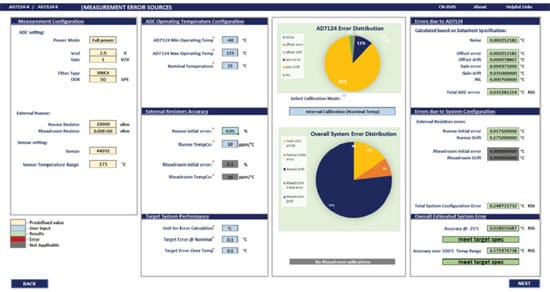
As observed in Figure 3, the error due to the ADC is not the significant error contributor to the overall system error. The external components along with their temperature coefficients or temperature drift specifications are usually the main error contributors across the system when operating at the full temperature range.
For example, if we change the sense resistor tempco from 10 ppm/°C to 25 ppm/°C in the tool, you will see that the overall system error will be significantly increased. Therefore, it is important to select the sense resistor with better initial accuracy and a lower temperature coefficient to minimize any possible temperature drift errors.
The AD7124-4/AD7124-8 offer different calibration modes that can be used to further reduce measurement errors. An internal calibration is recommended upon power up or software initialization to remove the ADC’s gain and offset errors at nominal temperature. Please take note that the tool uses a gain setting of 1. The AD7124-4/AD7124-8 are factory calibrated at a gain of 1 and the resulting gain coefficient is the default gain coefficient on the device. Therefore, the device does not support further internal full-scale calibrations at a gain of 1. Note that internal calibrations at nominal temperature remove the AD7124-4/AD7124-8 gains and offset errors only and not the gain and offset errors and any drift errors created by the external circuitry. Performing system calibrations can remove external errors. Performing calibrations at different temperature points can also improve drift performance. However, this will add additional cost and effort and may not be suitable for some of the applications.
Fault Detection
For any harsh environment or for applications where safety is a priority, diagnostics features are becoming more critical and even required. Even for nonsafe designs, diagnostics add robustness, ensuring that all blocks of the design are functioning correctly and the processor is receiving and acting on valid data only. The embedded diagnostics in the AD7124-4/AD7124-8 reduce the need for external components to implement diagnostics, resulting in a smaller, simplified, time and cost savings solution. Diagnostics include:
- Checks of the voltage level on the analog pins to ensure it is within the specified operating range
- A reference voltage check
- A cyclic redundancy check (CRC) on the serial peripheral interface (SPI) bus
- A CRC on the memory map
- Signal chain checks
- These diagnostics lead to a more robust solution.
Thermistor System Evaluation
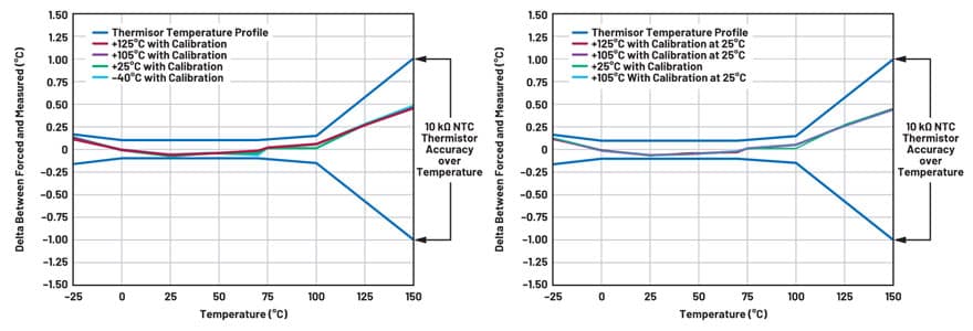
After conceptualizing the system design and understanding the expected system performance, the next step for a designer is to prototype and validate the performance of the design. CN-0545 is a Circuits from the Lab® reference design leverages EVAL-AD7124-4/EVAL-AD7124-8 evaluation boards and its evaluation software to provide measurement data for a 0.1°C accuracy thermistor. The circuit in CN-0545 uses a 10 kΩ, type 44031 NTC thermistor sensor, which is specified to measure from –50°C to +150°C with an accuracy of ±0.1°C between 0°C and +70°C and a ±1°C over the wider temperature range.
Figure 4 shows measurement results from CN-0545. This measured data was captured with the AD7124-4/AD7124-8 evaluation boards that include a thermistor demo mode that measures the thermistor resistance and calculates the equivalent °C using the sensor’s Steinhart-Hart constants. The plot shows the actual performance results. If you compare it to the error budget calculator, the actual results may appear better than the estimations provided by the tool. This difference is due to the tool using maximum values for all parameters, so it provides a worst-case analysis of the circuit. In practice, the sensor drift, initial accuracy, and temperature drift of the electronics and components used in the system will not always be at their specified maximum values.
Providing such flexible validated reference circuit boards is valuable to system designers as it lessens the design cycle and provides good circuit techniques. Along with the hardware, the software supports the different system optimization and calibration techniques for each thermistor sensor to meet the market demands where they need easy to use, high accuracy, precision, and reliable signal chain solutions.
Providing the designer tool and hardware demo mode circuit can ease the design process but system designers have different ways of handling measurements and may have used different controllers for software processing. To further ease the development process, a simple firmware application, AD7124 Temperature Measurement Demo Example, can be used to generate custom code with a choice of a controller board, a software platform, device configurations, and a measuring sensor such as a thermistor. This open source Mbed platform provides an ability to support over 150+ controller boards with or without modifications. Thus, it enables rapid prototyping and faster development phase.
Conclusion
This article demonstrated that designing a thermistor-based temperature measurement system is a challenging, multistep process. To ease the system designers’ journey, the Thermistor Configurator and Error Budget Calculator, along with Virtual Eval, the evaluation board hardware and software, Mbed firmware, and CN-0545 can be used to address the different challenges such as connectivity concerns and the overall error budget to bring users to the next level of their design.
Using highly integrated low bandwidth sigma-delta ADCs reduces the design effort further as they provide the building blocks needed to excite, condition, and measure the sensor along with eliminating concerns such as 50 Hz/60 Hz rejection.
This level of integration, along with the complete system collateral or ecosystem, will simplify the overall system design as well as the cost and design cycle from concept to prototyping.

