


Memristors are two-terminal resistor-like devices whose resistance depends on the history of current or voltage, providing non-volatile, analog or multilevel resistance states suitable for memory and neuromorphic computing applications.
They are implemented mainly as nanoscale resistive switching structures, most commonly based on metal oxides, enabling high-density integration and in-memory computing architectures.
Key Takeaways
- Memristors are two-terminal devices whose resistance depends on current history, enabling non-volatile memory and neuromorphic computing applications.
- They function as nanoscale resistive switching structures, primarily using metal oxides, allowing for high-density memory integration.
- The concept of memristors emerged from Chua’s theory in 1971, introducing them as the fourth fundamental circuit element alongside resistors, capacitors, and inductors.
- Memristors show unique behavior, such as nonlinear current-voltage characteristics and the ability to retain information after power loss, making them viable for various applications.
- They face challenges, including device variability and integration with existing technologies, but ongoing research suggests they will play a key role in future computing systems.
Concept and Theoretical Background
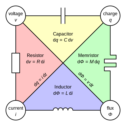
The memristor (memory resistor) was introduced by Leon Chua in 1971 as the fourth fundamental circuit element, complementing the resistor, capacitor, and inductor by linking electric charge and magnetic flux. In the ideal formulation, memristance is defined as the derivative of flux with respect to charge, , so that the instantaneous resistance of the device depends on the time integral of the current that has flowed through it. Under periodic excitation, an ideal memristor exhibits a pinched hysteresis loop in the current–voltage plane that passes through the origin and whose area shrinks with increasing frequency. At very high frequencies, the loop collapses to a straight line, and the device behaves like a linear resistor because the internal state cannot follow the fast excitation. This history-dependent behavior gives the memristor its characteristic ability to retain information in the form of a resistance value even after the bias is removed.
Electrical Symbol

Physical Realizations and Device Classes
Physical devices exhibiting memristive behavior were reported decades after the original theory, primarily in the form of nanoscale resistive switching cells. These devices are conventionally implemented as metal–insulator–metal (MIM) stacks, often referred to as resistive random access memory (ReRAM), which show reversible transitions between a high-resistance state (HRS) and a low-resistance state (LRS).
To encompass a broader range of realizations, the original notion has been generalized to “memristive systems,” where the device resistance depends on one or more internal state variables that evolve according to the applied stimuli. In practice, many devices termed memristors are resistive switching structures whose internal states reflect ionic concentration profiles, filament geometry, trapped charge, or polarization, rather than an ideal memristor. Even so, they are functionally exploited as non-volatile, stateful resistors that can store and process information in a compact form.
Materials Systems and Switching Mechanisms
A wide variety of material systems support memristive behavior, including binary and complex oxides, chalcogenides, perovskites, organic layers, and emerging two-dimensional materials. Common inorganic resistive layers include TiO, HfO, TaOx NiO, CuO, ZnO, WO, ZrO, and AlO, often combined with noble or conventional metal electrodes such as Pt, Ti, TiN, or TaN.
In many metal-oxide structures, resistive switching is attributed to formation and rupture of conductive filaments composed of oxygen vacancies or metal cations within the insulating matrix. Other devices rely on interface-type switching, where modification of Schottky barriers, charge trapping and detrapping, or ferroelectric polarization changes modulate the conductance. More recently, two-dimensional materials and layered heterostructures have been investigated to improve scalability, flexibility, and energy efficiency for neuromorphic computing.
Example: TiO2-Based Memristors
TiO-based nanostructured memristors were among the first widely discussed physical realizations, with early models describing drift of oxygen vacancies between a doped, conductive region and an undoped, insulating region. Depending on device geometry and bias conditions, these structures can exhibit digital-like switching for non-volatile memory or gradual, analog-like switching suitable for neuromorphic synapses. Variants such as nitrogen-doped TiOnanorods and mixed-oxide stacks have been explored to enhance switching uniformity, ON/OFF ratio, and endurance.
Electrical Characteristics and Figures of Merit
Memristors are characterized primarily by their current–voltage behavior and state-dependent resistance, typically showing nonlinear I–V curves with a pinched hysteresis under AC excitation. In addition to basic HRS and LRS values, many devices support intermediate resistance levels, enabling multilevel or analog storage. Important figures of merit include ON/OFF resistance ratio, switching voltage, switching speed, switching energy per event, retention time, endurance (number of switching cycles), and variability across devices and cycles. For memory applications, large ON/OFF ratios, low operating voltages, high endurance, and long retention at elevated temperature are critical. For neuromorphic use, additional priorities include smooth and symmetric conductance modulation, low write noise, and good reproducibility of analog weight updates.
Typical Memristor Characteristics
| Parameter | Typical range / behavior | Notes |
|---|---|---|
| ON/OFF resistance ratio | From to > depending on material | High ratios reported in optimized HfOx and TaOx devices. |
| Switching voltage | ~0.5–3 V | Lower voltages targeted for ultra-low-power neuromorphic operation. |
| Switching speed | ns to ms | Sub-ns speeds demonstrated in some HfOx and TaOx cells. |
| Endurance | – cycles | Material and stack dependent; TaOx can reach > cycles. |
| Retention | Up to 10 years (projected) | Evaluated at elevated temperature for non-volatile memory use. |
| Conductance states | 2 (binary) to tens–hundreds (analog/multilevel) | Number of stable states limited by variability and noise. |
| Energy per switching event | Down to sub-fJ–pJ per operation | Ultra-low energies reported for optimized neuromorphic devices. |
Device Modeling
Accurate memristor models are essential for circuit and system design. Analytical models derived from Chua’s original formulation describe memristance as a state-dependent resistance that evolves according to the applied current or voltage. Physics-based models incorporate ionic drift, redox reactions, filament growth and dissolution, and threshold phenomena to reproduce realistic I–V characteristics and switching dynamics. Piecewise linear and nonlinear window functions are often used to confine the internal state variable within physical limits and to capture boundary effects. For neuromorphic applications, models are further extended to reflect stochastic switching, device-to-device variability, and the pulse-dependent evolution of conductance for learning rules such as spike-timing-dependent plasticity.
Neuromorphic Computing and AI
Memristors are key enablers for neuromorphic computing architectures, where they serve as artificial synapses and, in some cases, artificial neurons. In crossbar arrays, memristor conductances represent synaptic weights, and Ohm’s and Kirchhoff’s laws naturally implement analog matrix–vector multiplication for neural network inference. This in-memory computing approach reduces data movement between separate memory and processing units, alleviating the von Neumann bottleneck and improving energy efficiency. Memristor-based synapses can implement essential plasticity mechanisms, such as long-term potentiation and depression, as well as more complex learning rules through suitable pulse schemes. Volatile memristors, including Mott and diffusive devices, can emulate neuronal dynamics such as leaky integrate-and-fire and spiking behavior, enabling compact hardware neurons for spiking neural networks.
Other Applications
Beyond neuromorphic computing, memristors are attractive for several additional application domains. In non-volatile memory, they are used as ReRAM cells in high-density arrays, where their small footprint and simple two-terminal structure enable multi-gigabit integration. Logic-in-memory and reconfigurable logic circuits exploit memristor states to perform Boolean operations and stateful logic directly where the data are stored. Memristor networks can also exhibit complex dynamical behavior, including chaos and self-organized patterns, which can be harnessed for random number generation, optimization, and unconventional computing schemes. Emerging material systems, such as GaO-based devices and flexible oxide stacks, open opportunities for harsh-environment electronics and conformal or wearable neuromorphic systems.
Challenges and Technological Outlook
Despite rapid progress, several challenges limit large-scale commercial deployment of memristor-based systems. Device variability, both from cycle to cycle and from cell to cell, complicates precise multi-level programming and reduces yield in dense arrays. Long-term retention under repeated analog updates, susceptibility to read and write disturbances, and reliability under temperature and voltage stress remain active research topics. On the integration side, controlling sneak-path currents in large crossbar arrays and ensuring compatibility with CMOS back-end-of-line processes are critical. From a system perspective, algorithm–device co-design is necessary to exploit the strengths of memristors while tolerating non-idealities, for example by using robust training schemes or redundancy. Continued advances in materials engineering, device design, and neuromorphic architectures suggest that memristor technologies will play an increasingly important role in edge AI accelerators, in-memory computing, and bio-inspired electronics.
Conclusion
Memristors extend the classical set of circuit elements with a history-dependent resistor that can inherently store information in its conductance state. Their nanoscale implementation as resistive switching devices provides a unique combination of non-volatility, multilevel programmability, and compatibility with dense crossbar arrays.
These properties make memristors strong candidates for next-generation non-volatile memories, logic-in-memory architectures, and neuromorphic computing hardware where computation and storage are tightly integrated. Although significant challenges remain in variability, reliability, and large-scale integration, ongoing research in materials, devices, and system architectures continues to close the gap between laboratory prototypes and practical products. As these issues are mitigated, memristors are expected to become key building blocks for energy-efficient, highly parallel computing systems that complement or extend conventional CMOS technology.
FAQ: Memristors
A memristor is a two-terminal non-linear resistor whose resistance depends on the history of current or voltage, allowing it to store information as a non-volatile resistance state.
Unlike a linear resistor with fixed resistance, a memristor exhibits history-dependent, nonlinear current–voltage characteristics and can retain its resistance value after the bias is removed.
Memristors are typically implemented as metal–insulator–metal stacks using metal oxides such as TiOx, HfOx, TaOx, NiOx, CuOx, ZnOx, WOx, ZrOx, and AlOx, often combined with electrodes like Pt, Ti, TiN, or TaN.
Key applications include high-density non-volatile memory (ReRAM), logic-in-memory architectures, and neuromorphic computing where memristors act as artificial synapses or neurons in crossbar arrays.
Memristors provide analog or multilevel conductance, local non-volatile weight storage, and highly parallel in-memory computation, making them ideal for implementing energy-efficient neural networks and brain-inspired hardware.
Typical characteristics include ON/OFF resistance ratios from about 10² to above 10¹⁰, switching voltages around 0.5–3 V, switching speeds from nanoseconds to milliseconds, endurance up to 10¹² cycles, and projected retention up to 10 years.
Thermistors and varistors are non-linear resistors whose resistance depends on temperature or voltage, respectively, while memristors are history-dependent devices that retain a programmable resistance state and can serve as memory elements.
References
[1] L. O. Chua, “Memristor – The Missing Circuit Element,” IEEE Transactions on Circuit Theory, vol. 18, no. 5, pp. 507–519, 1971.
[2] “Memristor,” Wikipedia entry (general overview of theory, history, and device types).
[3] S. S. et al., “Memristor Theory and Mathematical Modelling,” International Journal of Computer Applications.
[4] A. A. et al., “TiO2 Based Nanostructured Memristor for RRAM and Neuromorphic Applications: A Simulation Approach,” Nanoscale Research Letters.
[5] M. R. et al., “TiO2-Based Memristors and ReRAM: Materials, Mechanisms and Models,” arXiv preprint.
[6] Y. Wang et al., “A Review of Memristor: Material and Structure Design, Device Characteristics and Applications,” Nanotechnology and Precision Engineering, 2023.
[7] X. Liu et al., “Metal Oxide-Based Resistive Switching Memristors for Neuromorphic Computing,” Journal of Materials Chemistry C, 2025.
[8] H. Li et al., “Memristor-Based Artificial Neural Networks for Hardware Neuromorphic Computing,” Research, 2025.
[9] Y. Chen and G. Zhang, “Revolutionizing Neuromorphic Computing with Memristor-Based Artificial Neurons,” Journal of Semiconductors, 2025.
[10] X. Zhang et al., “Low-Power Memristor for Neuromorphic Computing,” Micromachines, 2025.
[11] EU Project “Tellurene Memristors for Neuromorphic Computing System-on-Chip,” CORDIS project ID 101187967.
[12] “Recent Advancements in 2D Material-Based Memristor Technology,” review of 2D memristive devices.
[13] “Gallium Oxide Memristors: A Review of Resistive Switching and Neuromorphic Applications.”
[14] “Emerging Higher-Order Memristors for Bio-Realistic Neuromorphic Computing: A Review.”
[15] “Recent Progress in Neuromorphic Computing from Memristive Devices to Neuromorphic Chips,” Advanced Devices & Instrumentation, 2024.
- https://passive-components.eu/memristors-key-to-nano-scale-analogue-digital-adaptive-hardware/
- https://passive-components.eu/new-memristor-boosts-accuracy-and-efficiency-for-neural-networks-on-an-atomic-scale/
- https://passive-components.eu/toward-brain-like-computing-new-memristor-better-mimics-synapses/
- https://passive-components.eu/first-programmable-memristor-computer-aims-to-bring-ai-processing-down-from-the-cloud/
- https://passive-components.eu/memristors-supports-brain-like-computing-system/
- https://passive-components.eu/purity-of-materials-may-be-the-key-in-further-memristor-development/
- https://passive-components.eu/nanometers-thin-niobium-oxide-nbo2-memristor-can-bring-breakthrough-in-neuromorphic-ai/
- https://passive-components.eu/graphene-based-memristors-show-promise-for-brain-based-computing/