
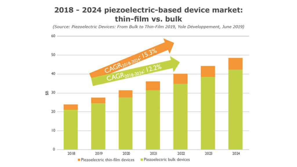
“The piezoelectric market for sensors, actuators, and transducers is expected to reach US$48.5 billion in 2024, with a 12.6% CAGR from 2018 – 2024 on comparable devices in bulk and thin-film technologies.» says Jérôme Mouly, Senior Technology & Market Analyst & Business Developer Yole Développement (Yole). « Thin-film piezo-based devices are driving the market’s growth, though market share is still in favour of bulk-based devices, which remains a strong technology in the piezo market ».
In both bulk and thin-film device markets, RF filters lead with SAW and BAW, respectively. Broadcom and Qorvo are the major thin-film players in the RF filters arena. 5G with an increasing number of frequencies will strongly boost the market. The recent fundraising efforts of consumer players like Amazon in thin-film-based companies to support the development of piezo microspeakers and MEMS piezo microphones confirm mainstream interest in technologies, explains Jérôme Mouly from Yole.
Such technologies are indeed able to work with ultra-low power. Bulk piezo devices offer the high actuation performance that is expected in a number of applications, from inkjet print heads to linear motors achieving very precise movements.
“Piezoelectric materials allow interactions between both worlds, electronic and mechanic,” explains Sylvain Hallereau from System Plus Consulting. “Actuator and sensor functions can be so directly integrated with electronic die. Today piezoelectric materials are so more and more used in modules.”
Specific to thin-film techniques, several MEMS foundries have internalized a thin-film piezo process in their fab. AlN requires extensive knowledge for piezo layer deposition, while PZT is an exotic material for integration in a semiconductor fab. In terms of deposition, two technologies are competing: Sol-Gel and PVD (sputtering or pulsed laser deposition – PLD). Sol-Gel offers better intrinsic film properties, with good uniformity and higher breakdown voltages. But when considering high volume production, throughput becomes a major consideration and this is where Sol-Gel exhibits limitations.
Most MEMS IDMs and foundries have already made their process choices. Fujifilm Dimatix and Robert Bosch have chosen sputtering, while Epson and Rohm Semiconductor will pursue Sol-Gel techniques. Yole’s analysts had the opportunity to debate with Robert Bosch and conducted a dedicated interview of Dr. Udo-Martin Gómez, Senior Vice President at Robert Bosch: The piezoelectric blessing is bestowed upon many MEMS devices.
“When we started the pre-development phase of piezoelectric MEMS, we made a thorough analysis of our application needs and compared this with the known deposition technologies, like Sol-Gel, PLD, Sputtering and others. In the end we decided on sputtering. Sputtering tools are well known in semiconductor fabs. The supply chain regarding sputter targets and other media is well established. This results in process and material properties which are under all circumstances controllable and reproducible even in high volume….” explains Dr. Udo-Martin Gómez from Robert Bosch.
Equipment manufacturers play an important role in developing the right process: for example, SolMAteS, a Netherlands-based equipment manufacturer, recently announced that its PLD technology has entered the next 5G base-station and receiver device market through a production site located in the USA…
All year long, Yole Group of Companies publishes numerous Manufacturing reports including the piezoelectricity reports collection. Yole’s experts realize various key presentations all year long.
Acronyms:
CAGR : Compound Annual Growth Rate
SAW : Surface Acoustic Waves
BAW : Bulk Acoustic Waves
RF : Radio Frequency
AlN : Aluminium Nitride
PZT : Lead Zirconate Titanate (piezoelectric ceramic material)
IDM : Integrated Device Manufacturer

