
Bourns has introduced the CDSOD323-TxxC-Q Series, an automotive‑grade bidirectional TVS diode family targeting ESD and surge protection on single high‑speed data lines and I/O ports in space‑constrained designs.
The TVS diode devices combine AEC‑Q101 automotive qualification, up to 30 kV ESD robustness and low capacitance in a compact SOD‑323 package, making them a practical alternative to larger multilayer varistors in modern automotive and consumer electronics.
Key features and benefits
- Bidirectional line protection – Single‑line TVS structure that clamps both positive and negative transient events on one data line or I/O pin, simplifying layout and BOM for differential and single‑ended interfaces.
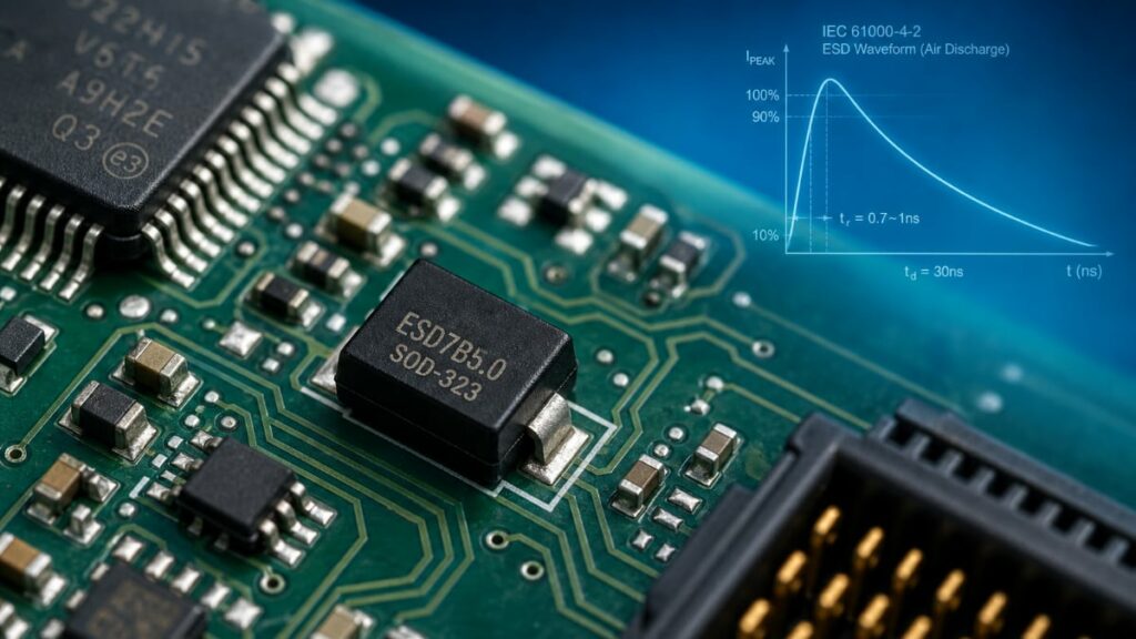
- High ESD robustness – Rated up to 30 kV according to IEC 61000‑4‑2, providing a wide protection margin for direct human‑body ESD events at external connectors, keypads, and exposed interfaces.
- Low typical capacitance (≈ 3 pF) – Supports high‑speed signal integrity where added capacitance would otherwise degrade eye diagrams or increase rise times, for example on USB or other fast serial links.
- Compact JEDEC SOD‑323 package – Small‑outline footprint supports dense PCB layouts in miniaturized ECUs and portable devices and fits standard pick‑and‑place and reflow processes.
- AEC‑Q101 qualification – Automotive‑grade screening for higher reliability across temperature and operating life, important for in‑vehicle infotainment, telematics, and sensor ECUs.
- Drop‑in MLV replacement option – Intended as a replacement for larger 0805 multilayer varistor components, helping engineers reduce footprint while maintaining or improving surge performance.
- RoHS compliant – Meets Bourns environmental compliance definitions, easing use in global designs without extra material approval work.
Typical applications
Although the series is automotive‑qualified, Bourns positions CDSOD323‑TxxC‑Q also for compact consumer and portable devices where board space and ESD robustness are both critical.
- Cellular phones and smartphones – Protection of audio jacks, buttons, RF control lines, side‑key interfaces, and baseband GPIOs exposed at connectors.
- PDAs and notebook computers – Protection of docking interfaces, SD card lines, and low‑speed control buses near user‑accessible connectors.
- Digital cameras, MP3 players and GPS devices – ESD protection on USB, memory card and accessory connectors in tightly packed enclosures.
- USB interfaces – General‑purpose USB data line protection, especially where low line capacitance and small footprint are more important than multi‑line integration.
- Automotive systems – Infotainment, telematics, body control, diagnostics connectors, and other automotive ECUs that require AEC‑Q101 components and compact protection for signal pins.
In practice, the devices are a good fit anywhere one or a few sensitive CMOS inputs are routed to a connector and cannot tolerate high parasitic capacitance or large discrete components close to the pins.
Technical highlights
The CDSOD323‑TxxC‑Q Series is a family of automotive‑grade TVS diodes; individual part numbers are differentiated mainly by their standoff and breakdown voltages, which must be chosen according to the interface signal levels. Exact voltage ratings, leakage specifications and clamp characteristics should be taken from the manufacturer datasheet.
Package and construction
- Package: JEDEC SOD‑323 plastic package.
- Polarity: Bidirectional configuration for protecting a single line in both polarities.
- Intended replacement: 0805 multilayer varistor in many designs, with reduced PCB area.
Electrical characteristics (overview)
The precise numbers depend on the selected TxxC‑Q variant and are according to the manufacturer datasheet, but the family includes:
- ESD capability: Up to 30 kV contact/air discharge (IEC 61000‑4‑2 test method).
- Typical capacitance: Approximately 3 pF, suitable for many high‑speed and RF‑sensitive lines that cannot tolerate higher‑capacitance TVS devices.
- Surge and EFT immunity: Designed to clamp surge and fast transient overvoltages on exposed signal lines.
Positioning versus multilayer varistors
Multilayer varistors in 0805 size are a common choice for single‑line ESD protection but consume more area and generally exhibit higher capacitance than a small‑signal TVS diode. Replacing an 0805 MLV with a CDSOD323‑TxxC‑Q device can:
- Reduce PCB footprint and allow denser connector pin‑field routing.
- Improve signal integrity where MLV capacitance was close to the limit for the interface.
- Maintain or improve ESD robustness as long as the selected TVS variant provides adequate clamping for the system‑level requirements.
Summary table: key characteristics
| Parameter | CDSOD323-TxxC-Q family (overview) |
|---|---|
| Protection type | Bidirectional TVS diode, single line |
| Package | SOD-323 (JEDEC) |
| ESD rating | Up to 30 kV (IEC 61000-4-2) |
| Typical capacitance | ≈ 3 pF (depending on type, see datasheet) |
| Automotive qualification | AEC-Q101 compliant |
| Intended MLV replacement | 0805 multilayer varistor in many signal-line applications |
Design‑in notes for engineers
When designing in the CDSOD323‑TxxC‑Q TVS diodes, treat them as protection elements that must be selected and placed carefully relative to the protected IC and the external interface.
- Choose the correct voltage variant – Select a TxxC‑Q type whose standoff voltage comfortably exceeds the maximum normal signal voltage, including tolerances, to avoid unwanted clamping during normal operation.
- Check clamping voltage against IC ratings – Use the datasheet surge and ESD clamping curves to verify that the maximum voltage at the protected pin under worst‑case surge is below the absolute maximum rating of the interface device.
- Place close to the connector – For best performance, place the SOD‑323 device as close as possible to the external connector or entry point and minimize the loop area between the TVS, connector pin and return path.
- Provide a solid return path – Ensure a low‑impedance ground reference (wide trace or plane) from the TVS diode to the system ground so that surge current is shunted away efficiently.
- Account for line capacitance – Although the typical capacitance is around 3 pF, high‑speed or RF interfaces may still require signal‑integrity simulation to confirm that the added capacitance is acceptable.
- Compare against existing MLVs – When replacing an 0805 multilayer varistor, compare surge energy ratings, leakage, and clamping behavior to ensure that the new TVS meets or exceeds current protection performance.
- Verify derating over temperature – For automotive environments, check the datasheet for any temperature dependencies in leakage current and clamping voltage across the full ECU temperature range.
Example use in an automotive ECU
A common use case is an automotive infotainment ECU where USB and auxiliary connectors are routed to a central SoC or USB hub:
- Use one CDSOD323‑TxxC‑Q device per differential pair line, placed adjacent to the connector footprints.
- Route short traces from the connector pins to the TVS pads and then to the main signal routes, avoiding long stubs.
- Tie the TVS return to the local chassis or digital ground reference near the connector to minimize common‑mode coupling into the rest of the system.
Source
This article is based on information provided in the official Bourns press release and associated product documentation for the CDSOD323‑TxxC‑Q automotive‑grade TVS diode series, with additional independent commentary for design engineers and component buyers.
References
- Bourns press release – Bourns Introduces CDSOD323-TxxC-Q Automotive-Grade TVS Diode Series for Compact ESD Protection
- Bourns CDSOD323-TxxC-Q Series – Product datasheet
- Bourns – Official website
Meta description:
SEO title: Bourns CDSOD323-TxxC-Q Automotive TVS Diode Series
Tags: Bourns, TVS diode, ESD protection, automotive electronics, AEC-Q101, transient voltage suppressor, multilayer varistor replacement, SOD-323, circuit protection, signal integrity
Featured image prompt: Close-up macro of a tiny SOD-323 TVS diode on a green automotive ECU PCB with visible fine signal traces, clean engineering style, abstract blue tech background with subtle ESD waveform overlay, sharp studio lighting with soft reflections on the package edges.

