
Würth Elektronik’s new WE‑FNCS flexible nanocrystalline sheets target exactly this need by providing a thin, easy‑to‑apply magnetic shield for enclosures and wireless power systems.
Nanocrystalline absorber sheets are an increasingly attractive option for shielding low‑frequency magnetic fields in compact electronic devices. They allow design teams to improve EMC compliance in the 10 Hz to 120 MHz band without resorting to complex metal can designs or mu‑metal parts.
Key features and benefits
- Flexible nanocrystalline absorber material
WE‑FNCS uses a nanocrystalline magnetic alloy with very high permeability to absorb low‑frequency magnetic fields rather than reflecting them. This helps reduce both emissions and susceptibility issues in sensitive circuitry. - Effective from around 10 Hz up to 120 MHz
The material targets the difficult lower frequency range where conventional shielding materials are often less effective, such as fields from transformers, common‑mode chokes, DC/DC converters, inverters and switched‑mode power supplies. - Scalable shielding performance via layer count
The absorber stack is built from multiple nanocrystalline layers whose number can be adapted. Increasing the layer count allows engineers to tune permeability and absorption performance to match specific problem frequencies and field strengths while keeping the overall construction thin. - Thin, highly flexible mechanical construction
The sheets are supplied as thin, bendable tapes and strips, enabling application on flat surfaces, curved housings or inside compact assemblies without major mechanical redesign. This also supports retrofitting during EMC troubleshooting. - Self‑adhesive, easy handling in production
An acrylic adhesive on the underside of the sheet allows simple peel‑and‑stick installation onto housings or shielded areas. Protective foils on both sides are removed only at the point of use, which helps avoid damage or contamination during handling. - Integrated insulation layer
A black PET cover layer provides electrical insulation on the top side, so the sheet can be placed against metallic housings or near conductive parts without additional insulating foils. This simplifies stack‑up and reduces assembly steps. - Custom formats and configurations available
Würth Elektronik offers WE‑FNCS in customized sizes and layer structures on request. This is helpful for OEMs that want pre‑cut pieces for specific device housings or optimized layer combinations for their target frequency range.
Typical applications
Low‑frequency magnetic fields from power and magnetic components can easily cause EMC test failures or interfere with sensitive circuitry. Typical use cases for Würth Elektronik WE‑FNCS include:
- Power electronics assemblies with transformers, common‑mode chokes or large inductors, where fields can couple into nearby control or communication circuits.
- DC/DC converter modules and compact power supplies in industrial, automotive or telecom environments requiring stringent EMC compliance.
- Inverters and motor drives where high currents and switching edges create stray magnetic fields around busbars, inductors and power stages.
- Hall effect sensors or other magnetically sensitive devices placed close to power components or busbars.
- Medical systems such as MRI‑related equipment, where shielding low‑frequency magnetic fields and controlling stray flux paths are important.
- Wireless power transfer systems, for example in consumer electronics or industrial devices, where the sheet can guide magnetic flux and reduce unwanted stray fields to improve coupling and overall efficiency.
In many of these applications, the flexible sheet format makes it possible to address EMC hot spots late in the design cycle by lining the inside of housings or shielding specific areas of a PCB or module.
Technical highlights
From an EMC and materials perspective, WE‑FNCS is positioned as a high‑performance low‑frequency magnetic absorber rather than a classical conductive shield.
Magnetic properties and frequency range
- High magnetic permeability due to nanocrystalline structure, supporting efficient absorption of low‑frequency magnetic fields.
- Designed for EMI attenuation roughly from 10 Hz up to 120 MHz, covering common mains‑related frequencies, switching converter harmonics and many wireless power transfer bands.
- Flux saturation levels suitable for practical shielding of fields generated by power magnetics in typical industrial, automotive and consumer designs (exact values according to manufacturer datasheet).
High permeability means that, for a given field, the material can “draw in” and dissipate magnetic energy, which reduces the field strength on the other side of the sheet. The broad usable frequency range is particularly useful where a single shield must cover both low‑frequency power components and higher‑frequency switching edges.
Mechanical and construction details
- Multilayer nanocrystalline core whose layer count can be tailored to the application, allowing a trade‑off between attenuation, thickness and cost.
- Black PET cover layer on the upper side, providing electrical insulation and mechanical protection.
- Acrylic adhesive layer on the underside for direct mounting to housings, covers or other surfaces.
- Both top and bottom surfaces protected by removable foils during storage and handling.
The PET cover layer helps maintain insulation distances and simplifies integration into existing mechanical designs, while the adhesive and protective foils support straightforward processing on the production line.
Product family overview
The WE‑FNCS family is offered as flexible sheets, tapes and strips. For detailed information on:
- Available standard sizes (sheet dimensions, tape widths and thicknesses).
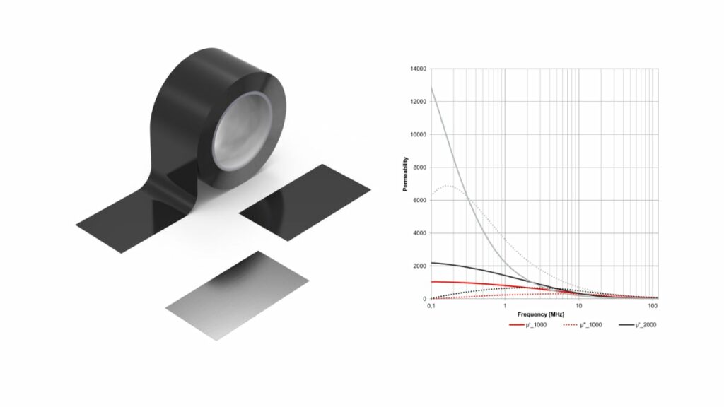
- Nominal permeability and attenuation curves across frequency.
- Maximum operating temperature and environmental ratings.
designers should refer to the official WE‑FNCS product and datasheet pages provided by Würth Elektronik. This avoids guessing values that may change as the portfolio evolves.
Availability and ordering options
Würth Elektronik positions WE‑FNCS as a standard catalog EMC component line with customization options.
Typical availability aspects:
- Standard sheets, tapes and strip formats suitable for prototyping and small‑volume builds.
- Custom‑cut shapes and tailored layer configurations available on request for series projects.
- Technical support offered by Würth Elektronik to help define suitable thickness, size and placement for specific EMC challenges.
When selecting part numbers, engineers and buyers should:
- Check the required sheet thickness and number of nanocrystalline layers based on targeted attenuation and available space.
- Verify temperature range and environmental ratings in the datasheet for the intended application (e.g. industrial control, automotive, medical).
- Ensure that chosen formats match the mechanical design (e.g. pre‑cut rectangles for housing walls, long strips for shielding along PCB edges).
If distributors or purchasing systems do not list every variant, it can be helpful to work directly with Würth Elektronik to define custom configurations.
Example parameters to consider
Although exact part numbers and ratings are best taken from the manufacturer datasheet, the table below summarizes typical selection parameters for flexible absorber sheets like WE‑FNCS.
| Parameter | Design consideration |
|---|---|
| Sheet thickness | Must fit mechanical stack‑up while providing sufficient attenuation |
| Permeability / layer count | Higher permeability or more layers for stronger fields or lower frequencies |
| Sheet size / shape | Should cover the main field path or coupling area without unnecessary oversizing |
| Adhesive type and strength | Must withstand operating temperatures and mechanical stress in the end application |
| Operating temperature range | Needs to meet or exceed the device’s specified ambient and self‑heating levels |
Engineers should cross‑check these parameters with the official WE‑FNCS product documentation before freezing a design.
Design‑in notes for engineers
- Identify dominant field sources and victims early
During layout and mechanical design, map where transformers, chokes, busbars and inductors sit relative to sensitive analog, measurement or communication circuits. This will guide where WE‑FNCS sheets can make the most impact. - Use near‑field probing in the lab
During EMC troubleshooting, scan the device with magnetic near‑field probes to locate hot spots. Apply test strips of WE‑FNCS in these areas to quantify the achievable reduction before committing to cut parts or tooling. - Optimize layer count versus thickness
For strongly coupled low‑frequency sources, a single thin layer may not provide sufficient attenuation. Consider parts with more nanocrystalline layers or stacking multiple sheets where space permits, balancing shielding effectiveness against mechanical constraints. - Pay attention to mechanical integration
Ensure that the PET‑insulated side faces any conductive parts where insulation is required. Avoid trapped air gaps and ensure good contact of the adhesive side to the housing surface to prevent vibration or peeling in the field. - Consider thermal aspects
While absorber sheets are typically not primary thermal paths, they can influence airflow or contact between components and housings. Check that adding WE‑FNCS does not inadvertently block necessary cooling paths or create hot spots. - Plan for manufacturability
For series production, consider specifying pre‑cut shapes delivered on a roll or in panels to reduce manual cutting. Clear assembly instructions should show orientation (PET side vs. adhesive side) and exact placement location. - Use shielding together with good layout practice
WE‑FNCS should complement, not replace, good EMC design: minimize loop areas, optimize return paths, and place sensitive traces away from strong magnetic field sources wherever possible.
Source
The information in this article is based on the official Würth Elektronik press release on the WE‑FNCS flexible nanocrystalline sheet product line and associated manufacturer documentation.
References
- Würth Elektronik press release – Quick and Easy Shielding (WE‑FNCS)
- Würth Elektronik WE‑FNCS product overview

