
This technical article written by Ron Demcko, KYOCERA AVX discusses ESD suppression methods using multilayer MLCC ceramic capacitors or MLV varistors and provide its selection guide for automotive applications.
Introduction
Due to the enhanced complexity of the automotive applications, one could easily argue that automotive ICs are now more susceptible than ever to transient voltages. Designers commonly utilize shielding and routing methods to reroute transients, transient voltage suppressors to clamp the effects of incoming transients, or integration capacitors to capture transient voltages etc.
However, no single methodology provides the perfect solution for every automotive application due to their various cost, size, and capability limitations. This article identifies performance differences between multilayer varistors and multilayer ceramic capacitors utilized in ESD suppression applications.
Modern-day automobiles utilize incredible amounts of computing power to create a constantly improving transportation experience. As a result, transportation is safer, more enjoyable, and more efficient than ever. The electronics that enable these improvements are evolving in a few key ways. First, sensors and dedicated processing units are observing and acting on more data than ever before, spanning environments ranging from cabin electronics to under-hood modules. Next, several central processing units are sending data on high-speed networks to even larger and more powerful processors that profile, prioritize, and control sub systems. Finally, automobiles are talking to both one another and infrastructure via RF links.
Due to the enhanced complexity of the enabling silicon devices behind the scenes, as well as the critical importance of their reliable performance, one could easily argue that automotive ICs are now more susceptible than ever to transient voltages. Designers commonly utilize shielding and routing methods to reroute transients, transient voltage suppressors to clamp the effects of incoming transients, or integration capacitors to capture transient voltages and slowly release their energy back into the circuit at levels below the susceptibility limit. However, no single methodology provides the perfect solution for every automotive application due to their various cost, size, and capability limitations.
This article identifies performance differences between multilayer varistors and multilayer ceramic capacitors utilized in ESD suppression applications. In it, design approaches are compared using IEC 61000-4-2 standards, and are tested for ESD surge and survivability, EMC filter capability, and EFT/surge survivability and effectiveness. This article also examines the effects of ESD on high-speed signal lines and the long-term reliability of each device, and compares EMC filtering characteristics through the use of S21 parameters.
Cost Considerations
With regard to efficacy, the ideal method of transient voltage suppression is to clamp the transient voltage with a transient voltage suppressor (TVS). Of all the TVS devices available on the market, multilayer varistors (MLVs) are one of the best choices due to the fact that they are small, lightweight, and capable of both clamping voltages in their on-state and acting as an EMI filter in their off-state. However, this level of protection, and the cost associated with it, is not necessary for every lower level automotive application.
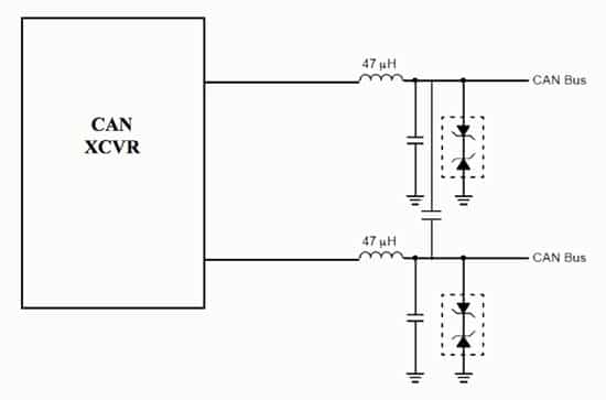
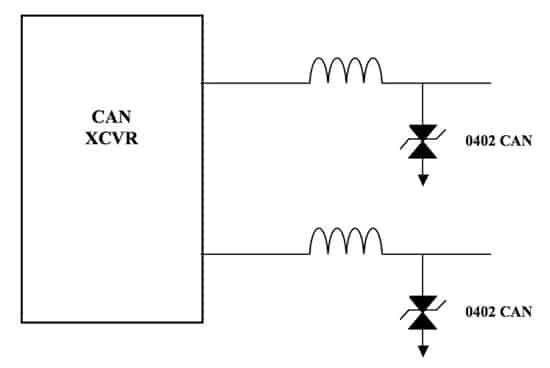
MLVs are, however, particularly ideal for use in communication circuitry, such as controlled area networks (CANs). Modern vehicles have several dozen CAN interfaces that require transient control. A typical CAN circuit, both before and after the implementation of CAN MLVs, is shown in Figure 1. In this example, an MLV is connected from both the CANH and CANL lines to ground, and is used to provide EMI filtering in the off-state of the varistor and to protect the IC in a bidirectional fashion when ESD or other transients are present. As such, the MLV is an effective replacement for the EMC capacitor, as well as the bidirectional diodes used in the circuit with a single MLV. MLVs are also well suited for use in auto CAN circuits due to the fact that they can operate at 150°C without the need for de-rating. So, as CAN interfaces and other communication buses continue to expand their roles to under-hood applications, the case for the use of MLVs will only become greater.
For automotive applications employing lower cost, slower, and less complicated ICs with at least a moderate degree of inherent ESD survivability, the combination of a PCB layout optimized for input/output ports and MLCCs capable of surviving exposure to ESD voltages may offer an effective solution for protecting ICs from ESD events. The key to employing this method is understanding that it is only effective in the case of short waveforms incidents upon fairly rugged ICs in non-critical applications that can withstand large amounts of capacitive loading. Luckily, though, that combination of qualities isn’t all that uncommon. Within any common engine control unit (ECU), there is typically an 80/20 need for ESD integration capacitors vs. MLVs on the pins. So, assuming that the most common ECUs have 300 pins, that means a 240:60 ratio of integration capacitors to MLVs.
ESD Models
Electrostatic discharge (ESD) is a sub-nanosecond rise-time event that is generated by the charge transfer of materials in the tribo-electric material series. ESD can be either positive or negative in polarity, contact- or air-discharge, and repetitive or random in nature.
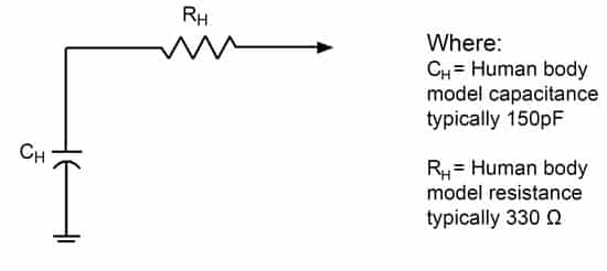
An ESD event is typically modeled by a capacitor charged to a particular voltage level in series with a current-limiting resistor, both of which are discharged at particular repetition rates to simulate a certain number of real-world transients on the device under test (DUT). There are several models that can be used to simulate the various transient sources that could inject ESD into a victim, but the three most common are the charged device model (CDM), the machine model (MM), and the human body model (HBM).
This article concentrates on the IEC 61000-4-2 HBM (150pF, 330Ω) in contact discharge mode, a configuration of which is shown in Figure 2. Although there are many common transients that are slow in speed, this article only considers fast transients due to the fact that MLCCs will charge to the level of the driving voltage in the case of the slowest transients, which provides no assistance for semiconductors that need to survive transient threats.
Transient Voltage Control via Clamping With Multilayer Varistors (MLVs)
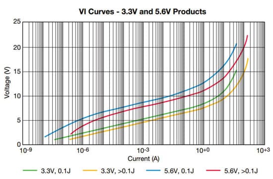
Multilayer varistors are zinc oxide (ZnO2) based ceramic semiconductors that exhibit nonlinear voltage-current (VI) characteristics in the presence of an electric bias. The number of grains between the multilayer conducting electrodes determines the breakdown voltage, which is defined as the 1mA current conduction point on the VI curve. Clamping voltage is defined as the maximum voltage measured with an 8×20µs waveform applied at a specific current magnitude defined by the energy rating of the part. Another parameter of MLVs is operating voltage, which is the steady-state voltage that can be indefinitely applied to the MLV without causing an increase in the specified leakage current of the part.
The VI curve for a multilayer varistor is pictured in Figure 3, which illustrates that MLVs are TVS clamps. MLVs offer advantages over other TVS clamps, such as diodes, and significant advantages over MLCCs. These MLV advantages include large in-rush current capabilities, high-energy transient suppression, and off-state bulk EMC capacitance. Further, when coupled with an extremely low FIT rate and ease of assembly, these benefits make MLVs an attractive device for modern circuit protection.
Transient Voltage Control via MLCC Integration
Many transient voltage control designs utilize a capacitor at the I/O pin to integrate the voltage and thereby protect the IC from ESD damage. Although this can be an effective design practice, engineers often overestimate the capacitor’s performance due to the capacitor’s significant value drop upon the applied ESD event.
Generally speaking, the amount of capacitance drop for NP0 dielectrics is negligible. However, the amount of capacitance drop for X7R capacitors can be 50% or greater. Furthermore, this value varies from manufacturer to manufacturer, as well as on a lot-by-lot basis within any particular manufacturer, as ESD voltage coefficient is not characterized on a lot-by-lot basis for standard capacitors.
The capacitance drop from the expected value of a standard X7R capacitor can result in a much higher voltage at the IC or device that needs to be protected. ESD capacitors can be an effective weapon in the control of ESD events, but designers should exercise extreme care during the device selection process.
Consider this. The conservation of charge applies to the capacitance voltage product of the ESD model and the combined capacitance of the ESD model + the ESD integration capacitor.
This can be represented by:
Cmodel * Vmodel = (Cmodel + Cicap) * Vic
where
- Cmodel = the capacitance of the ESD model
- Vmodel = the voltage to which the model is charged
- Cicap = the capacitance value of the integration capacitor
- Vic = the voltage that the IC (or device to be protected) sees
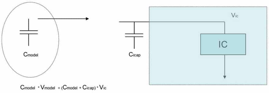
The original charge of the ESD model used is split between the ESD model’s capacitance and the ESD integration capacitor. For example, if the ESD model capacitor is 150pF and charged to 8kV, and the integration capacitor is 1,000pF, the expected surge voltage at the IC would be approximately 1,044V. However, if we assume the 1,000pF has a 50% drop in capacitance, the voltage that the IC is subjected would actually be 1,846V. As such, NP0 dielectrics used to be a more common dielectric choice in transient voltage control designs since they do not require designers to consider the effects of ESD voltage coefficients. However, the emergence of ESD-safe MLCCs is changing that concern, and allowing smaller case size integration capacitors to miniaturize designs.
The X7R dielectric is widely employed in transient voltage control applications in which designers can maximize capacitance for a lowered ESD integration voltage that is acceptable at the IC. This approach might be acceptable in some cases, but data skew can easily occur depending on the rate of data transmission. In other cases, designers try to optimize the PCB layout by placing the most sensitive ICs deep within the PCB and relying on the traces’ series inductance and parallel capacitance to further reduce the transient threat.
One application that is ideal for the equivalent of long PCB traces with sensitive ICs placed away from the transient is the case of a wiring harness interfaced with a PCB module. So, we conducted tests with this in mind to generate comparative ESD HBM performance data.
ESD Capacitor vs. MLV HBM ESD Testing
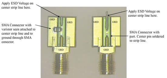
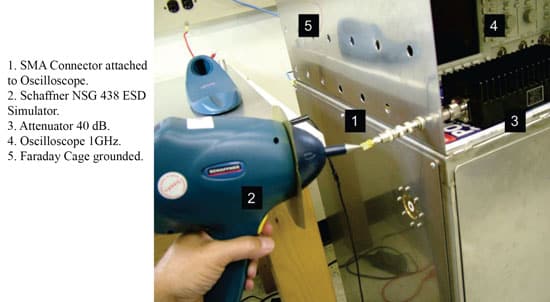
Human body model (HBM) ESD tests were performed on two common MLCCs and an MLV in an effort to determine the effect of each device on an IEC 61000-4-2 ESD waveform of varying magnitude. In this test, the device under test (DUT) was soldered to a test card terminated with an SMA connector that connected to an entry port on a faraday-shielded 40dB attenuator that connected to a TDS 784 oscilloscope.
Test set-up and definition is shown in Figures 5 and 6.
The test proceeded with the contact discharge of positive and negative transients of 2kV, 4kV, and 8kV ESD strikes to the DUT. The resulting voltages captured are representative of the ESD voltage magnitude at the port of the device to be protected. The series of graphs pictured in Figures 7, 8, and 9 illustrate the relative protection of a 4.7nF X7R dielectric MLCC, a 100nF X7R dielectric MLCC, and an 18V MLV, and the difference between integration and clamping devices.
The 2kV graph (Figure 7) shows the effect of positive and negative waveforms on all three of these devices. Both types of devices — the MLCCs and MLV — are non-polar, so the graph is symmetrical. As the transient voltage is increased, so is the integrated voltage of the MLCC. Alternately, the MLV has a relatively constant clamping voltage regardless of the ESD transient magnitude.
These tests illustrate that larger value capacitors will integrate the transient voltage to a lower voltage level. However, as stated earlier, there is a practical limit to the amount of capacitance loading that a circuit may allow. Voltage lines have no capacitance limit, while signal and data lines have a concrete value of capacitance with which they can be loaded before experiencing signal degradation.
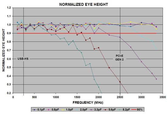
Eye diagrams are useful tools for determining the maximum allowed capacitance loading on a device in need of ESD suppression. The graph pictured in Figure 10, which shows the effect of capacitance on the eye height of USB and PCI-E circuits, provides evidence that large value ESD capacitors cannot be used to effectively clamp transient voltage.
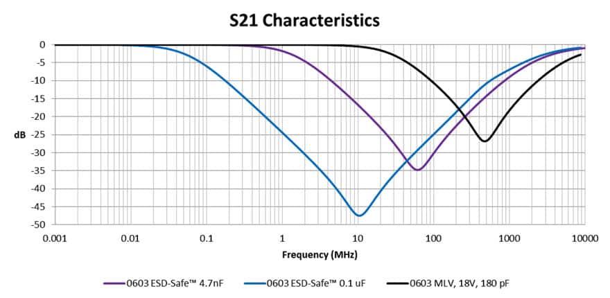
However, from a frequency response perspective (Figure 11), ESD-capable MLCCs are just as effective for off-state EMI filtering as MLVs, and ESD-Safe™ capacitors come in an extremely wide range of capacitances when compared to MLVs.
The following table depicts the range of commonly available ESD capacitor and MLV sizes.

Summary
To study the efficacy of transient voltage protection devices in both in-cabin and under-hood automotive applications, we confirmed a test method for ESD testing based on a faraday-shielded storage scope, attenuator, and industry-standard ESD simulator.
Our tests confirmed that — although ESD capacitors are not practical in high-speed circuitry or circuitry with a large fan-out (e.g., sensors, high-speed communication ports, and audio/video signals) due to capacitive loading, and are also ineffective against slow-speed transients, which require a clamping device, like an MLV — ESD capacitors are effective transient control devices for ICs that are relatively ESD-hardened when subjected to single-shot ESD events with long series inductance.
In fact, ECUs commonly employ standard MLCCs as integration capacitors for roughly 80% of their pins, and the introduction of ESD-Safe™ MLCCs provides designers with a wider selection of MLCCs with higher reliability results.
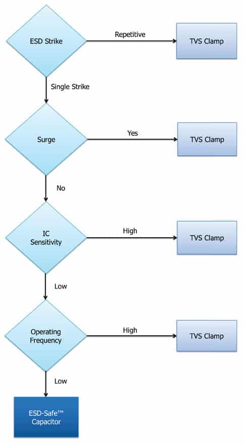
A flowchart for effective automotive ESD protection selection based on these results is pictured in Figure 13.
References
Dr. Eran Jones, “Sub-pF Varistor Application Model: Capacitance on High-Speed Circuits,” AVX Advanced Product and Technology Center.

