
Source: Nanotechweb.org news
Low dielectric constant (or low-k) materials are promising for faster, smaller and higher performance electronics devices. However, most low-k materials available today are very porous, which makes them mechanically weak and unstable at high temperature. A team of researchers in the US and Korea has now made a 3D nano-architectured dielectric material based on alumina that does not suffer from these problems. The structure might be used to make devices such as capacitors, wide-band antennas and stable wiring for high-voltage applications in aerospace and hydrogen vehicles.
Manufacturing the nanolattice capacitor
“We fabricated 3D nano-architectured hollow-beam alumina dielectric capacitors with a k of 1.09–1.10 that is stable over the –20 to +20 V range and the 100 kHz to 10 MHz range,” explains team leader Bong Joong Kim of the Gwangju Institute of Science and Technology (GIST) in Korea. “The devices have extremely small dielectric losses of just 0.01–0.1 and the dielectric material itself has excellent mechanical properties, namely a Young’s modulus of 30 MPa, a yield strength of 1.07 MPa and an outstanding thermal stability with a thermal coefficient of the dielectric constant of 2.43 × 10⁻⁵/K up to 800°C.”
Designing and synthesizing low-k materials is important because they can be used in applications like computer processing components, wireless communications and automotive radar, he adds. Lowering the k of the interlayer dielectric in such devices decreases the resistance–capacitance (RC) delay, reduces power consumption and lowers cross-talk between nearby interconnects – all of which are serious problems in modern integrated circuits (ICs).
Lowering the k of a material
A low-k is also good for multi-chip module (MCM) technology, which allows passive elements like inductors, resistors and capacitors (which serve as building blocks in 3D circuits for microwave/millimetre wavelength communications) to be integrated into devices. For example, the antenna in a typical radio-frequency module for radiating and receiving radio waves requires a supporting substrate with a k that is sufficiently low to prevent surface propagation of the waves and to increase bandwidth.
One way to lower the k of a material is to introduce porosity into it, since the k of air is very low. However, the problem here is that increased porosity often leads to poorer mechanical and thermal properties, and unstable electrical properties. This is because it is difficult to control the size of pores and how they are distributed in a material.
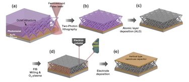
Making a 3D ceramic nanolattice
Kim and colleagues made their low-k dielectric by depositing a gold/titanium bottom electrode on a highly-doped silicon substrate. The gold part of the electrode measures 80 nm and the titanium part 12 nm. Next, the researchers deposited a photoresist on the top of the electrode and then directly wrote a nanolattice scaffold into the photoresist layer using a technique called two-photon photolithography direct laser writing.
“We then coated this polymer nanolattice with a 10 nm-thick conformal layer of alumina (Al2O3) using atomic layer deposition and etched the photoresist away in oxygen plasma using a focused ion beam. Finally, we evaporated an identical Au/Ti (80/12 nm) bilayer as a top electrode on the top plate of the nanolattice to create a parallel plate capacitor.”
“Our 3D ceramic nanolattice might be used to create faster, smaller and higher performance microelectronics devices that consume less power, for computer processing components, wide-band antennas and stable wiring for high-voltage applications in aerospace and hydrogen vehicles,” he tells nanotechweb.org.
The team, which includes researchers from the California Institute of Technology in the US, led by Julia Greer, says that it is now trying to vary the design of the nanolattice to improve the overall physical and electrical properties.
The research is detailed in Nano Letters DOI: 10.1021/acs.nanolett.7b03941.

