

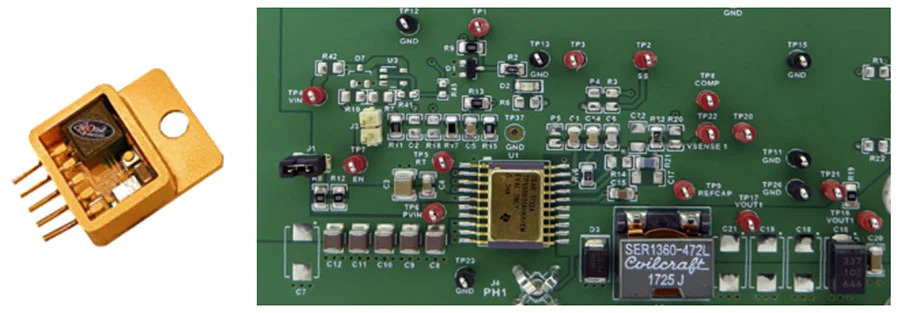
With the increasing use of low-voltage, high-current loads such as FPGAs within spacecraft avionics, engineers are increasingly having to design-in switching-mode regulators to generate supply rails. Selection of passive electronic components is one of the key item for reliable operation. Dr. Rajan Bedi, CEO and founder of Spacechips, discuss its selection guide in article published by EDN.
Most of the qualified parts have integrated the switching and low-side FETs, but require an external inductor as well as input and output capacitors. The choice of these passives is very important as they determine the quality of the conversion, i.e. input and output ripple, load regulation, and response to single-event effects (SEEs).
Power supply design is by its very nature full of trade-offs and compromises such as cost, size, performance, and reliability. However, there is also scope to optimise and reduce the dimensions and mass of the energy-storing passives.
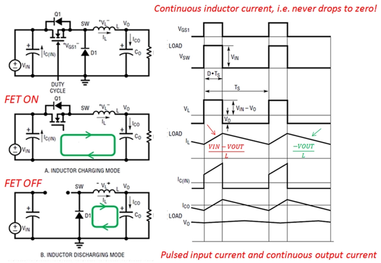
Switching DC-DCs regulate the output voltage based on energy flow into and from the DC-DC by controlling the duty cycle of the on and off states. When the switch is conducting, energy flows from the input source into the convertor and in the case of a buck, some of this gets stored in the inductor as magnetic energy (0.5*LI2) while some gets delivered directly to the output (forward topology). Similarly, during the off interval, energy is delivered from the convertor to the load. For a buck, this comes from the inductor, where it was previously stored when the FET was on.
The energy added to the inductor during the on-time is always equal to that delivered to the load when the switch is off, i.e. the inductor ends each cycle with exactly the same current and energy it started with; the definition of steady state!
As an example, assuming a switching frequency of 500 kHz, an input of +5.5V, a load voltage of +0.95V, a load current of 18 A, and a conversion efficiency of 90%, the resulting input and output powers are 19 and 17.1 W respectively. The source energy drawn during each switching cycle is 38 µJ and the energy output when the FET is off is 34.2 µJ. At a frequency of 500 kHz, the total energy processed by the regulator is 17.1 J/s, or 17.1 W by definition.
When we add energy to an inductor, the current through it ramps up linearly. When we remove the energy, current ramps down, resulting in an observed ac current ripple. In an analogous manner, when we add energy to a capacitor, the voltage across it ramps up linearly. When we remove the energy, voltage ramps down, resulting in an observed ac voltage ripple. The switching action continuously adds and removes energy, producing current ripple through the inductor and voltage ripple across capacitors. For both, there are guidelines for the maximum amount of tolerable ac variation relative to its dc level.
For a buck regulator, the inductor stores the input energy in its magnetic field when the switching FET is on and delivers this to the load when the high-side transistor is off. The choice of the value of inductance is based on the level of current ripple to be delivered to the load, defined by a geometrical ratio, r:
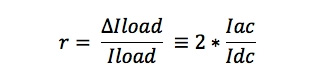
where Iload is the average inductor current, ΔIload is the current swing, Iac and Idc are the ac and dc values of the inductor current respectively. The resulting inductance in Henrys related to r can be calculated from:
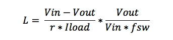
where fsw is the switching frequency in Hertz.
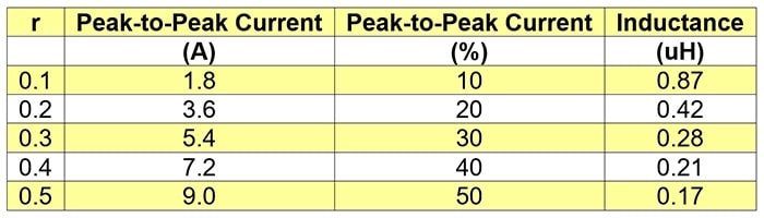
For example, to generate a +0.95V rail at 18 A, the following table lists the absolute peak-to-peak inductor current ripple in amps and as a percentage of Iload, as well as the resulting inductance as a function of r:
The value of the inductance is inversely proportional to load current and switching frequency while its physical size and mass are proportional to Iload.
A fully-integrated, space-grade buck regulator offers an overall smaller form factor and is easier to design-in, while having to add an external magnetic and passives gives the designer more control over the level of current ripple, and hence the voltage variation passed to the load.
A large inductance produces less current ripple, resulting in lower voltage fluctuation in the load. A larger inductance, because of its natural tendency to oppose a change in current, slows the transient response of the regulator and increases power loss due to a bigger intrinsic dc resistance. A smaller inductance improves the speed of regulation but increases the amount of output ripple and risks the inductor being driven into saturation. It is important that the inductors’ rms current and saturation current ratings are not exceeded, with the latter greater than the calculated peak value. The physical size of the magnetic must match its energy-handling capability and a bigger core is required to handle higher powers. Please also check the tolerance of the inductance, which can vary by up to 30% for some suppliers, resulting in higher than desired ripple current.
The inductor current ripple appears as a variation in the output voltage and one of the functions of the output capacitance is to reduce the amount of ripple seen by the load. Capacitor ESR and ESL are important parameters that determine the output voltage ripple associated with the inductor current.
A capacitor naturally resists changes in ac. voltage and once it is charged, has a tendency to maintain the voltage, especially if there is ripple riding on top of the dc. The capacitor, if appropriately sized, will be too slow to keep up with voltage fluctuations due to ripple, so they get filtered out.
When the FET is off, the input is disconnected from the output, however, the load will always require a continuous flow of energy. During this time, the output capacitance must also store sufficient charge to provide the load an output: when the switch is off, the inductor current decreases while supplying the load and the output capacitance buffers this current variation so the load sees a nearly constant voltage.
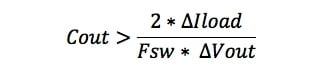
The output capacitance also determines how the regulator responds to a large change in load current. It must be sized appropriately to supply the load while the DC-DC cannot and until the latter’s feedback control loop is able to respond. The following equation specifies the minimum output capacitance necessary to accomplish this:
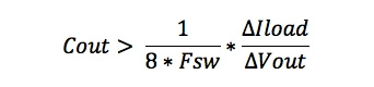
while the following equation calculates the minimum output capacitance to meet the target output voltage ripple requirement:
The LC filter formed by the inductor and output capacitance removes the ac component of the switching waveform to output an average (dc) voltage. For a buck regulator, the output capacitance is repeatedly charged and discharged by the ripple centred on the load voltage. Trace Ico in Figure 1 plots the continuous current flowing into the output capacitance.
Typically a variety of different capacitors are used in parallel to minimise the equivalent series resistance (ESR) and equivalent series inductance (ESL) contributions to output ripple as well as current sharing to ensure reliable operation. Parts are chosen based on their rated ripple current, working voltage, and parasitics.
Figure 3 plots the ripple-voltage contributions generated by ESR, ESL, and capacitance. The ESR contribution is resistance * current, the capacitance component is the integral of current and time, producing triangular waves, and the ESL component can be expressed as a derivative, with an instantaneous spike occurring at each switching instant producing high-frequency, pulse-like noise. The total voltage fluctuation across the capacitor comprises a composite sum of these three components:
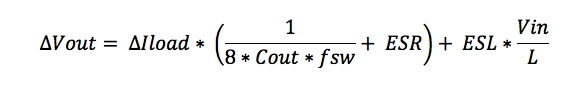
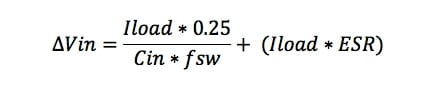
The peak-to-peak voltage ripple seen at output is inversely proportional to capacitance and switching frequency, but proportional to load current, ESR, and ESL.
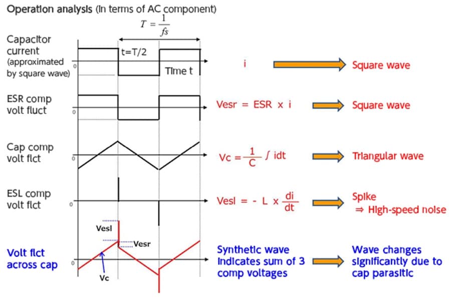
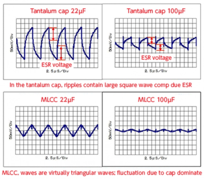
Figure 4 compares the ripple voltage measured from tantalum and multi-layer ceramic capacitors (MLCCs). MLCCs have lower intrinsic ESR and increasing the amount of capacitance reduces ripple further.

Input capacitance reduces the source ripple voltage seen at the switch of the DC-DC to a level that can be handled by the bulk capacitors without impacting the latter’s ESR dissipation. For a buck regulator, the ac part of its input current is supplied by the capacitance when the FET is on and conducting. When the high-side switch is off, the input capacitance recharges and trace Ic(IN) in Figure 1 plots its discontinuous, trapezoidal waveform with high di/dt and peak-to-peak amplitude. The source is not able to generate such a rapidly-changing pulsating current.
Bulk input capacitance is used to minimise source voltage deviations to ensure a stable output during load transients. The higher the capacitance, the lower the perturbation, which is directly proportional to changes in load current.
A good starting place to determine the amount of input capacitance is to specify the target level of peak-to-peak voltage ripple, which is inversely proportional to capacitance and switching frequency, but proportional to load current and ESR:
For a buck regulator, the input capacitor’s rms current is much higher than that in the output capacitor and the former is determined by its stress requirements, whereas on the output, it is simply the maximum allowed load ripple that determines the amount of capacitance. The largest, permissible rms current for a capacitor can be calculated from its maximum power consumption, derived from its case size, ESR, and the tolerable temperature rise.
Typically, a variety of different capacitors are used in parallel to minimise the ESR and ESL contributions to the input ripple as well as current sharing to ensure reliable operation. Parts are chosen based on their rated ripple current, working voltage, self-heating, ESR and ESL, with multi-layer ceramics used because of their low parasitics. The observed ripple, therefore, is almost entirely due to the actual capacitance and attention must be paid to thermal and dc bias effects on the value of capacitors. Dielectrics, which are less sensitive to temperature, are typically used to minimise changes in capacitance. The higher the temperature, the lower the reliability, including lifetime.
There are many trade-offs when designing a buck regulator: a higher switching frequency reduces the level of ripple voltage in the input and output capacitors as well as decreasing the amount of capacitance required by the DC-DC. However, reducing the latter increases the amplitude of the voltage ripple and switching at a faster rate increases ac losses, impacting efficiency. There are also opportunities for optimisation, e.g. for a given voltage ripple target, capacitance can be decreased provided the switching frequency is increased to avail of smaller energy-storage components.
A smaller inductance has lower DCR, improves transient response, and less output capacitance is required for a given transient performance. A larger inductance results in lower ripple current hence less capacitance is required for an equivalent output ripple.
If the inductor’s saturation current is exceeded, its inductance will drop, increasing the ripple current: a 30% drop in inductance will increase ripple current by > 40% as well as saturating the core. Shielded inductors reduce EMI and potential interference but are slightly more expensive because of increased manufacturing costs. Shielding tends to lower the saturation current which in turn lowers the maximum allowable rms current. Lsat also varies with temperature!

