Fundamentals of Inductive Switching and RC Snubber Impact
This is the first of the two articles devoted to the topic of an RC snubber design. In Part I we discuss the fundamentals of the inductive switching and the need for circuit protection. The impact of an RC snubber and snubber capacitor on the circuit performance is demonstrated through a series of simulations. Part II (to appear in the March 2019 issue of In Compliance) will address the systematic process of the snubber circuit design, together with the simulation and verification through the laboratory measurements. Writtten by Bogdan Adamczyk and Bill Spence.
Switching in an Unprotected Inductive Circuit
Consider the circuit shown in Figure 1(a). When the switch is closed, in steady-state the voltage across the inductor, vL, is zero, and a dc current I0 flows through the inductor. The energy stored in the magnetic field of the inductor is
When the switch opens, a large negative voltage develops across the inductor and subsequently the switch. The magnetic energy stored in the inductor is dissipated in the arc across the switch contacts or is radiated, as shown in Figure 1(b).
This behavior is often destructive to the switch and some sort of a protective circuitry is required. Before introducing a possible solution (RC snubber) let’s augment the circuit of Figure 1 with the stray capacitance of the wiring, as shown in Figure 2.
When the switch is closed, in steady-state no current flows through this capacitance. When the switch opens, the inductor’s current now flows through the stray capacitor charging it, and the voltage across it rises at an initial rate of . When this voltage exceeds contact breakdown voltage, an arc occurs across the switch contacts [1], and the capacitor discharges. When the arcing stops the current charges the capacitor again potentially causing another arcing.
The electrical oscillations occurring in this LC resonant circuit when the switch is opened are often the source of the voltage transients and high-frequency emissions. The voltage and current transients often manifest themselves as the ringing waveforms, like the one shown in Figure 3 [2].
These oscillations can be reduced by placing a snubber across the switch, as shown in Figure 4.
There are many different kinds of snubbers; this paper focuses on the most widely used – an RC snubber. The RC snubber design discussed here is used in a step-down or buck SMPS.
A typical buck SMPS schematic with an RC snubber across the low-side FET is shown in Figure 5.
Figure 6 shows the same buck SMPS with the parasitic capacitances and inductances explicitly shown [3].
The impulse voltage generated at the switching node stimulates the parasitic components to resonate as a damped LC network. The purpose of the RC snubber placed across the low-side switch is to reduce these oscillations to an acceptable level.
RC Snubber Impact
The basic resonance frequency in an RLC network is [4],
The resonant frequency in a circuit shown in Figure 6 , without a snubber in place, is
A simple circuit demonstrating this behavior is shown in Figure 7.
A close-up of the ringing waveform shown in Figure 8, reveals the ringing frequency of 412.9 MHz.
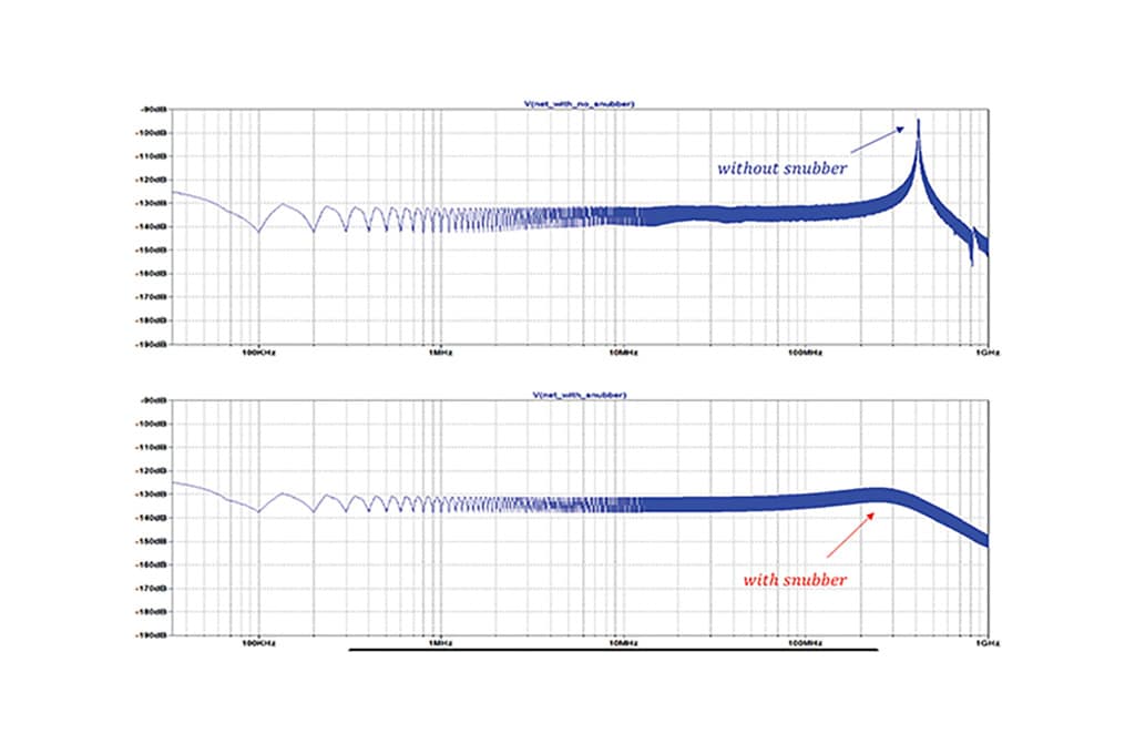
FFT of the ringing waveform is shown in Figure 9.
To move the resonant frequency to a lower value a 150 pF capacitor is added between the switching node and reference, as shown in Figure 10.
The resulting ringing waveform is shown in Figure 11.
Note that the ringing frequency has been reduced from 412.8 MHz to 206.7 MHz.
Using a snubber capacitor-only is generally not recommended [1]; to limit the discharge current of the snubber capacitor (and protect the switch) a resistor if often placed in series with the capacitor.
Figure 12 shows a full RC snubber circuit, with a 7.5 Ω resistor added.
The resulting ringing waveforms are shown in Figure 13.
Note that the resonant frequency increased from the capacitive snubber value in Figure 11 but is still much lower than that of the un-snubbed circuit.
Figures 14 and 15 clearly show the dramatic improvement of the RC-snubbed circuit response compared to the un-snubbed one.
Continue reading:
- RC Snubber Design for SMPS Protection Part II
- Filtering Capacitors for Switch Mode Power Supplies
- Guide to Snubber Capacitors
References
- Henry Ott, Foundations of Electromagnetic Compatibility Engineering, Wiley, 2009.
- Bogdan Adamczyk, “Circuit Theory Model of Ringing on a Transmission Line,” In Compliance Magazine, November 2018.
- Bill Spence, “Snubber Design: Reducing SMPS EMI,” Lunch and Learn, Gentex Corp, 2014.
- Bogdan Adamczyk, Foundations of Electromagnetic Compatibility with Practical Applications, Wiley, 2017.
Dr. Bogdan Adamczyk is a professor and the director of the EMC Center at Grand Valley State University (http://www.gvsu.edu/emccenter) where he performs research and develops EMC educational material. He is an iNARTE certified EMC Master Design Engineer, a founding member and the chair of the IEEE EMC West Michigan Chapter. Prof. Adamczyk is the author of the textbook “Foundations of Electromagnetic Compatibility with Practical Applications” (Wiley, 2017). He can be reached at adamczyb@gvsu.edu.
William Spence is a Senior Electromagnetic-Compliance Engineer and has been working in Gentex Corporation’s Electro-Magnetic-Engineering Lab for the last fifteen years. Previously, Bill was a Senior Microphone Design Engineer at Electro-Voice, Inc., where he worked for twenty-four years. Bill’s name has been listed in a dozen U.S. Patents for automotive microphone, digital communications, and switch-mode-power-supply designs. He frequently presents seminars on EMC/ESD topics and microphone design. Bill can be reached at bill.spence@gentex.com.
