




Large voltage spikes are common in power circuits, especially during switching. Switching devices are exposed to large spikes during turn-off, and voltage suppression circuits are required to protect them.
Snubber capacitors control switching transients by providing a local path for transient current and storing energy while an associated network limits voltage overshoot or damps ringing. This guide explains snubber circuits, capacitor construction and selection, and practical RC and flyback RCD-clamp calculations for design, component and purchasing engineers working with power converters, inverters and motor drives.
Key Takeaways
- A series RC snubber damps a parasitic resonance; a flyback RCD clamp limits voltage by steering transient current into a capacitor with a parallel discharge resistor. Their resistor calculations are not interchangeable.
- Select snubber capacitors for actual voltage, dV/dt, peak current, RMS current, ESR, ESL and temperature conditions, not capacitance and DC voltage alone.
- Polypropylene film is a common choice for repetitive pulse duty. Class 1 ceramic capacitors are also useful in compact, fast-switching power stages; neither technology should be selected solely from converter power.
- In an input-rail-referenced flyback RCD clamp, the capacitor voltage must exceed the reflected output voltage. The MOSFET drain clamp level is approximately the input voltage plus the capacitor voltage, with additional diode and layout-related contributions.
- Flyback clamp dissipation can substantially exceed leakage-inductance energy multiplied by switching frequency, particularly when the capacitor voltage is close to the reflected output voltage.
- Short connection loops and representative waveform measurements are essential. A snubber cannot compensate fully for excessive commutation-loop inductance or an unsuitable component package.
Snubber Circuits
Snubbers are networks used to control switching transients. Depending on their connection and operating principle, they can limit voltage overshoot, reduce ringing, control dV/dt, reshape a switching trajectory or move dissipation from a semiconductor into another component. They are not automatically required in every converter, and a dissipative snubber does not automatically improve total efficiency. [1]
Hard switching exposes a device to overlapping voltage and current during transitions. Package inductance, PCB interconnections, transformer leakage inductance, junction capacitance and other stray capacitances can produce additional overshoot and oscillation. Buck, boost, buck-boost and inverter circuits share some switching-network features, but their current paths, voltage levels and snubber requirements are not identical.
Layout and EMI considerations
The snubber must act on the current loop responsible for the unwanted transient. Place its capacitor, resistor and any steering diode close to the relevant device terminals or commutation path, using short connections with a small loop area. A connection that is short on the schematic can still have excessive inductance on the assembled board.
Use suitable planes or short, wide conductors and avoid unnecessary connection length. Keep high-dV/dt nodes and high-di/dt loops away from sensitive control, gate-drive and measurement circuits. The capacitor’s own ESL, package geometry and mounting arrangement form part of the snubber loop; increasing capacitance without considering these factors may not improve the fastest part of the transient. [1]
Waveforms and stored energy
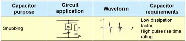
Inductor current cannot change instantaneously. When a switch interrupts a current path, current commutates into available capacitances, diodes, clamps or another branch of the circuit. Without an adequate path, voltage can rise until semiconductor avalanche, insulation breakdown or contact arcing provides one.
The energy EL stored in an inductance L carrying current I is given by Eq. (1). For a flyback leakage-energy calculation, L is the primary-referred leakage inductance and I is the current at the start of the relevant turn-off transient.
A capacitor stores energy rather than dissipating it ideally. Its transient current iC, capacitance C and terminal voltage vC are related by Eq. (2). This relationship explains why capacitor selection must include both voltage slew rate and pulse-current capability.
The change in stored capacitor energy, ΔEC, between an initial voltage V1 and a final voltage V2 follows Eq. (3). The initial voltage matters: absorbing a given energy into an already charged capacitor is not equivalent to charging an initially uncharged capacitor.
Equating EL in Eq. (1) to ΔEC in Eq. (3) provides an initial energy-storage estimate only when the assumed current path actually transfers that energy into the capacitor. It does not establish damping, total circuit loss or peak voltage in a network containing nonlinear semiconductor capacitances and significant connection inductance. [1]
Types of snubber circuits
The names C, RC and RCD describe component combinations, but the schematic connection determines their behavior. In particular, a local DC-bus capacitor, an RC network across a switch and an RCD flyback clamp perform different functions even though each may be called a snubber.
- C snubber: a capacitor provides a local transient-current path or limits voltage rise. A local capacitor across a half-bridge DC supply is not equivalent to an added capacitor directly across an individual switch, which may discharge through that switch at turn-on.
- RC snubber: a resistor and capacitor connected in series form a damping branch across a switch, diode or other ringing node. The resistor dissipates transient energy and limits capacitor discharge current.
- Discharge RCD snubber: a diode creates different charging and discharging paths. In a common turn-off arrangement it bypasses the resistor during capacitor charging, while the resistor controls discharge. The diode does not eliminate all loop impedance or all losses.
- Non-discharge RCD snubber or clamp: the capacitor retains a substantial voltage between switching events, and the resistor removes the energy accumulated during clamping. A conventional flyback RCD clamp is an important example, although its exact connections differ from some bridge snubber arrangements.
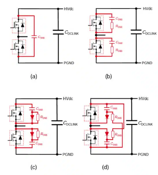
Figure 2 illustrates these distinctions in bridge circuits. Do not apply a resistor equation from one arrangement to another without checking the charging path, discharging path and voltage across each component. A conventional resistor-dissipative RCD network is not an energy-recovery circuit merely because its return connects to a supply rail. [1]
IGBTs, silicon MOSFETs and SiC MOSFETs can all require transient control. The appropriate switching frequency and snubber arrangement depend on device losses, switching conditions, thermal limits and the surrounding circuit. There is no universal frequency threshold or converter-power boundary that separates RC applications from RCD applications.
Snubber Capacitors
A snubber capacitor is selected for its role in a transient-control network, not simply for a nominal capacitance and voltage. The important stresses include repetitive peak voltage, voltage reversal where present, dV/dt, peak current, RMS current and internal temperature. Film, ceramic and mica technologies offer different combinations of capacitance, stability, pulse capability and package inductance.
Film capacitors for snubber applications
Polypropylene is widely used for pulse and snubber capacitors because of its low dielectric loss and relatively stable capacitance. However, the film material alone does not establish pulse capability: electrode thickness, winding arrangement, internal series sections, end connections and terminals also matter.
Metallized film constructions can provide self-healing, in which a localized dielectric breakdown clears a small area of metallization. Conventional film/foil constructions use discrete metal-foil electrodes and do not provide the same self-healing mechanism, but can offer high pulse-current capability. It is therefore incorrect to classify film/foil capacitors generally as suitable only for low-pulse applications.
Hybrid and double-metallized constructions combine features of different electrode arrangements. Their performance must be established from the particular series specification rather than inferred from the word hybrid. Self-healing capability is not permission to exceed repetitive pulse or thermal ratings.
Dedicated snubber series may offer PCB leads, multiple terminals or mounting lugs for direct connection to power modules. As an example of the parameters available in a manufacturer’s specification, KEMET’s C4BS datasheet lists separate voltage, ripple-current, peak-current, ESR, ESL and dV/dt ratings, together with mounting geometries. Its voltage range includes 1 kV, 2 kV and 3 kV DC options; these are product-family examples, not universal snubber requirements. [2]
Polypropylene capacitors are also used in resonant circuits, pulse discharge, coupling, precision timing and other applications. A general-purpose film capacitor intended for one of these functions is not automatically qualified for the repetitive waveform of a particular snubber.
Ceramic capacitors for snubber applications
Class 1 ceramic dielectrics, particularly C0G/NP0, provide stable capacitance and low loss without the pronounced DC-bias dependence and ferroelectric aging associated with Class 2 materials. Small surface-mount packages can also support short, low-inductance connections, making suitable Class 1 parts useful for high-frequency damping networks.
Ceramic capacitors are not restricted to low-power converters. High-voltage C0G products and mechanically relieved metal-terminal constructions are used in power-electronic applications, including on-board chargers and large-current snubber circuits. The relevant distinction is whether a particular part meets the electrical, thermal and mechanical requirements, rather than the total output power of the converter. [3]
Class 2 ceramics can provide more capacitance in a given volume, but their effective capacitance depends on applied voltage, temperature and aging. If one is used in a snubber, calculations must use its effective operating capacitance, and waveform-dependent heating must be checked. A nominal capacitance measured under small-signal conditions is not sufficient evidence of suitability.
MLCCs also require attention to board flex, soldering stress and thermal cycling. Flexible or metal-terminal constructions can reduce transferred mechanical stress, but the complete assembly and mounting process still require validation.
Choosing between film, ceramic and mica
Use polypropylene film when the required capacitance, repetitive pulse energy, RMS current and available mounting arrangement favor it. Use an appropriately rated Class 1 ceramic when compact size, low connection inductance and stable small capacitance are particularly important. Mica can be useful where stable capacitance and low high-frequency loss are required, but its pulse and current capability must also be confirmed for the selected product.
For all three technologies, compare impedance over the frequency range of interest rather than relying only on an ESR value quoted at a low test frequency. A large capacitor can be ineffective against the fastest ringing if its ESL and mounting inductance dominate the branch impedance.
Application examples
The same component technologies appear in several converter classes, but the design objective changes with the circuit. A damping network across a buck switch node, an RCD clamp in a flyback converter and a capacitor at an inverter module must each be analyzed using their actual current paths.
RC damping in SMPS switching nodes
A series RC network across a ringing switch or rectifier is intended primarily to dissipate oscillatory energy. For a simplified effective inductance Lp and capacitance Cp, the undamped natural frequency f0 is given by Eq. (4). Measured ringing frequency approximates this value only when damping and nonlinear effects are sufficiently small.
A practical starting method measures the original ringing frequency and then repeats the measurement with a known additional capacitance Cadd connected across the same ringing node. If f1 is the lower frequency with Cadd fitted, Eq. (5) estimates the effective parasitics. The method assumes that the added component does not materially change the participating inductance or the resonant mode. [6]
Choose an initial snubber capacitance Cs large enough to couple the ringing energy into the damping resistor, while keeping switching loss acceptable. A commonly used starting point is around three times Cp; adding that capacitance directly across the node would approximately halve the natural frequency in the ideal LC model. It is a tuning method, not a universal minimum capacitance. An initial resistor Rs near the parasitic characteristic impedance is given by Eq. (6). [6]
The measured example in the SMPS design reference uses 476.1 MHz before adding capacitance and 294.1 MHz after adding 68 pF. Recalculation with Eq. (5) gives Cp ≈ 42.0 pF and Lp ≈ 2.66 nH. Three times Cp is approximately 126 pF, and Eq. (6) gives approximately 7.97 Ω. The reported implemented network is 150 pF and 7.5 Ω, demonstrating that calculated starting values are subsequently adjusted and verified in hardware. [6]
Do not describe Eq. (6) as a universal critical-damping equation. The series RC branch interacts with the original parasitic capacitance, distributed interconnections and device capacitances. Tune resistance and capacitance while observing both switching edges, peak voltage, ringing decay and component temperature.
For a capacitor that experiences a complete voltage excursion of magnitude ΔV on each of two transitions per switching period, the idealized charge-and-discharge loss is approximately Eq. (7), where fs is switching frequency. The estimate assumes sufficient settling between transitions and does not include every other loss mechanism in the converter.
Eq. (7) follows from the one-half Cs(ΔV)² dissipated during each complete resistive voltage transition. Use the actual capacitor voltage excursion, not an unrelated bus or device rating. In circuits with incomplete settling, asymmetric transitions or multiple ringing events, integrate resistor power over the measured or simulated switching cycle instead.
SMPS primary snubbers and flyback RCD clamps
In flyback and forward converters, leakage inductance can create turn-off overvoltage at the primary switch. A flyback RCD clamp commonly connects a diode from the drain node to a capacitor and parallel resistor referenced to the positive input rail. It is distinct from a series RC network directly across the MOSFET. [4, 5]
During flyback switch on-time, energy is stored in the magnetic circuit while the secondary rectifier is reverse-biased. At turn-off, useful magnetizing energy transfers to the secondary. Leakage-related current cannot commutate instantaneously into the secondary path and instead drives the initial drain-voltage rise.
The clamp diode conducts when the drain voltage exceeds the input rail plus the clamp-capacitor voltage and diode forward voltage. Current charges the capacitor during this interval; the parallel resistor removes the accumulated energy. With sufficiently small capacitor ripple, the capacitor can be treated as an approximately constant voltage during the brief clamping event. [5]
Define the flyback voltages before calculating
Let Vin be the input voltage, Vout the output voltage, VF,sec the secondary rectifier forward voltage and n = Np/Ns the primary-to-secondary turns ratio. The reflected secondary voltage Vref during secondary conduction is approximately Eq. (8). For synchronous rectification, use the corresponding secondary conduction drop instead.
Define VC as the voltage across the clamp capacitor and its parallel resistor, measured relative to the positive input rail. It is not the drain-to-source voltage. During clamping, the drain-to-source voltage VDS,clamp is approximately Eq. (9), where VF,clamp is the clamp-diode forward voltage. Additional overshoot can arise from diode dynamics and connection inductance.
The required condition is VC > Vref. Comparing the total drain clamp voltage directly with Vref misses the voltage reference and can give an invalid design. If VC is too low, the clamp can conduct during the intended secondary energy-transfer interval rather than only during leakage-current commutation. [4, 5]
Derive the flyback clamp resistance and power
Let Llk be the primary-referred leakage inductance and Ipk the current entering the clamp interval. Assume a nearly constant VC, a nearly constant Vref, negligible diode drop for the calculation and an approximately triangular clamp current. The voltage driving leakage-current decay is VC − Vref, giving the approximate clamp duration tc in Eq. (10).
The charge Qc delivered through the diode in one clamping event is the triangular current area. With Elk = LlkIpk²/2, Eq. (11) follows.
In periodic steady state, the capacitor has zero net charge change over a switching period. The average clamp-diode current therefore equals the average resistor current IR,avg. For one comparable clamp event per switching period, Eq. (12) relates that current to the clamp resistance Rc.
Combining Eqs. (11) and (12) gives Eq. (13). The average resistor dissipation PR is VC²/Rc, producing the equivalent power expression in Eq. (14). These are the standard small-ripple flyback RCD-clamp relationships. [4, 5]
Eq. (14) shows why using only fsElk can underestimate clamp loss. During current commutation, the primary winding also has a reflected voltage across it. In this simplified model, the additional energy term per event is VrefQc; it is associated with energy diverted during the transformer’s energy-transfer process. It should not be described simply as input-voltage power added to the resistor.
As VC approaches Vref, the calculated current-decay time and loss increase sharply. The divergence identifies a limit of both the design and the approximation: the transient can no longer be treated as a brief event with unchanged current and reflected-voltage conditions. Conversely, increasing VC reduces the idealized loss multiplier but raises MOSFET voltage stress.
The result is a starting model, not a guarantee of final peak voltage or dissipation. Device output capacitance, transformer capacitance, finite magnetizing inductance, diode behavior and distributed inductance can change the current entering the clamp and the resulting waveform. Validate the design over the actual operating range. [5]
Choose the flyback clamp capacitor
The capacitor must retain enough voltage between clamping events for the small-ripple assumption to remain useful. If Cc is clamp capacitance and ΔVC,pp is the target peak-to-peak ripple, the approximate relationship in Eq. (15) follows from resistor discharge between short charging events. [5]
Eq. (15) assumes a clamp interval short relative to the switching period and small ripple. Check the minimum capacitor voltage against Vref, and the maximum capacitor voltage against component and MOSFET stress limits. Increasing capacitance reduces ripple, but it does not independently determine the average clamp voltage, which also depends on resistance and transferred energy.
Check capacitor pulse current separately from ripple. The diode delivers a short charging-current pulse, while the resistor provides a different discharge-current waveform. The capacitor’s RMS current is therefore not equal to the average resistor current in Eq. (12).
Worked flyback examples and design trade-offs
In Sam Ben-Yaakov’s simulation, the flyback operates at approximately 100 kHz and a duty ratio of 0.4, with a 30 V input and 1 µH primary-referred leakage inductance. The reported unclamped drain waveform reaches approximately 150 V for a nominally 100 V MOSFET model. With the clamp connected, the drain level is approximately 55 V. These are results from that simulation, not general device ratings or measured production margins. [4]
Ignoring diode drop for the comparison, Eq. (9) gives VC ≈ 55 V − 30 V = 25 V. The secondary inductance in the ideal coupled section is one quarter of the primary inductance, corresponding to a primary-to-secondary turns ratio of two. With approximately 10 V output and rectifier drop neglected, Eq. (8) gives Vref ≈ 20 V. [4]
The capacitor-voltage headroom is therefore only 5 V. Substitution in Eq. (14) gives a loss multiplier of 25/(25 − 20) = 5. Thus, under the simplified assumptions, resistor dissipation is five times fsElk. The example illustrates why a low clamp-capacitor voltage can be thermally expensive even when the nominal drain-voltage level appears comfortably below the MOSFET rating.
The original energy example in this guide uses 1 µH leakage inductance and 5 A turn-off current. Eq. (1) correctly gives 12.5 µJ. For an illustrative extension of that example, combine these values with 100 kHz switching frequency, VC = 25 V and Vref = 20 V. This extension does not assert that the video simulation uses 5 A.
The leakage-energy rate is then 1.25 W. Eqs. (10), (13) and (14) give a clamp interval of approximately 1 µs, a calculated resistance of 100 Ω and resistor dissipation of 6.25 W. Selecting a resistor only for 1.25 W would therefore be inadequate for this idealized case. The 1 µs interval is also long enough relative to the 10 µs switching period that the short-interval approximation deserves explicit verification.
For a 5% peak-to-peak capacitor-ripple target in the same illustrative case, ΔVC,pp is 1.25 V. Eq. (15) gives an initial Cc estimate of 2 µF. This is a first-order calculation, not a final component recommendation: the finite charging interval, actual effective capacitance, pulse current, temperature and voltage extrema must be checked.
For a fixed clamp-voltage target, higher leakage inductance or peak current requires a lower resistance and increases dissipation. A higher selected capacitor voltage permits a higher resistance and lowers the idealized loss multiplier, but reduces the available MOSFET voltage margin. Transformer leakage reduction, clamp voltage and semiconductor rating must therefore be considered together.
Inverter and motor drive snubbers
In inverters and motor drives, local capacitors can reduce the commutation-loop inductance seen by an IGBT or MOSFET module, while RC or RCD branches address residual switching transients. Device-level snubbing and DC-bus decoupling are related but distinct functions. The connection points determine which inductance is bypassed or included in the transient loop. [1]
Long motor cables introduce additional distributed effects. A network intended to control local semiconductor overshoot should not be assumed to solve motor-terminal reflected-wave stress or every cable-related EMI problem. Evaluate those effects at the relevant terminals and with the actual cable configuration.
For fast-switching SiC stages, package and interconnection inductance can be as important as nominal capacitance. Coordinate snubber design with gate-drive settings, local bus decoupling and device voltage margin; simply transferring an older IGBT snubber value to a different switching arrangement is not sufficient. [1]
High-frequency resonant converters
Soft switching does not eliminate all local parasitic ringing. A damping branch may still be useful around a rectifier, switching node or other localized resonance. However, an added capacitor can also change commutation charge, resonant behavior and the conditions required for soft switching.
In LLC and other resonant converters, distinguish a protection or damping capacitor from the deliberately designed resonant-tank capacitor. Verify operation across load and input conditions rather than treating added capacitance as a loss-free improvement.
Design and selection checklist
Begin with a waveform and a clearly identified current path. A component specification should describe what the snubber must withstand repetitively, including abnormal operating conditions that the equipment is required to survive.
Capacitor datasheet parameters
- Capacitance: nominal value, tolerance and effective value at operating voltage, temperature and frequency. Include aging where relevant to the dielectric.
- Voltage: DC bias, repetitive peak, AC component, voltage reversal and temperature-dependent limits. Do not substitute a one-time test voltage for a repetitive operating rating.
- Pulse capability: permitted dV/dt, repetitive peak current, pulse duration and repetition rate. Check the relationship between dV/dt and current using Eq. (2).
- RMS current and heating: current spectrum, ESR at relevant frequencies, permissible temperature rise and cooling conditions. A peak-current rating does not establish continuous thermal capability.
- ESL and mounting: terminal geometry, connection length, impedance behavior and the installed current-loop area. Compare the actual package, not only the dielectric technology.
- Environment and life: ambient and hotspot temperature, humidity, vibration, mounting stress, expected capacitance change and manufacturer endurance conditions.
Resistor and diode checks
For an RC damping resistor, compare pulse-energy capability, repetitive pulse loading, peak voltage, average dissipation and parasitic inductance. A sufficient average wattage rating alone does not demonstrate survival of short, high-amplitude pulses. Resistance changes both ringing and the capacitor-current waveform, so verify the selected physical resistor in the circuit.
For a flyback RCD clamp, the resistor is across the clamp capacitor and sees approximately VC, not the full drain-to-source voltage. Check average power from Eq. (14), voltage rating, thermal derating and overload behavior. If several resistors share the load, verify their voltage and thermal distribution rather than assuming ideal sharing.
Select the clamp diode for reverse voltage, repetitive current, peak current, forward recovery, reverse recovery and junction temperature. Its dynamic behavior and the clamp-loop inductance can create an initial voltage spike before the capacitor establishes the intended clamp level. [1, 5]
Catalog versus custom parts
A catalog part is preferable when its published electrical limits, terminal arrangement and environmental specification meet the application. Custom termination spacing or a purpose-designed assembly may be useful when a standard package leaves excessive loop inductance or does not fit the power-module geometry.
For either route, give the supplier the complete voltage and current waveforms, repetition rate, operating temperature, cooling arrangement and required life. Request confirmation of repetitive duty where the datasheet does not define it. Do not treat equal capacitance and voltage markings as evidence that two parts are interchangeable.
Qualification and safety
Check the qualification and reference standards claimed for the exact series and ordering code. For example, the C4BS specification references IEC 61071 for power-electronic capacitor applications; this is a series-specific statement, not a claim that every snubber capacitor has identical qualification. [2]
Application approval must also cover the final connection. A high DC voltage rating alone does not establish suitability for a mains-connected suppression or insulation-related position. Confirm the required safety approvals, creepage, clearance, discharge provisions and failure containment for the equipment and its intended installation.
Reliability, testing and derating
Snubber performance must be verified electrically and thermally. The objective is not merely an attractive oscilloscope trace, but acceptable semiconductor stress, component temperature, repetitive endurance and EMC performance throughout the required operating range.
Measure the relevant waveform
Measure at the protected device terminals using a probe arrangement with suitable voltage rating, bandwidth, common-mode performance and low connection inductance. A long probe connection can add apparent ringing, while probe capacitance can change the circuit being measured. Keep the measurement arrangement consistent when comparing candidate snubbers.
For an RC network, compare both switching edges, ringing amplitude, decay and resistor temperature. For an RCD clamp, measure drain voltage, capacitor voltage and ripple, diode-current duration and resistor dissipation. Confirm that the diode stops conducting after the intended commutation event rather than diverting substantial energy during the normal secondary-conduction interval.
Do not select the final network solely to move an FFT peak to a lower frequency. Check peak voltage and ringing decay as well as the conducted and radiated emissions relevant to the equipment. A local waveform improvement does not by itself demonstrate EMC compliance.
Test operating extremes and failure mechanisms
Test input and load extremes, startup, shutdown, load transients and relevant fault-recovery conditions. In a flyback converter, maximum steady-state load is not necessarily the only critical condition: startup and output-short recovery can expose the switch and clamp to different peak currents and voltages. [7]
Apply the manufacturer’s voltage, current and temperature limits to the actual waveform. Where resistor loss is inferred from voltage, use cycle-averaged squared voltage divided by resistance; the square of average voltage is only an adequate approximation when ripple is small. Where capacitor loss is estimated from ESR, use frequency-appropriate loss data and confirm temperature rise.
Potential failure mechanisms include dielectric breakdown, metallization or end-connection damage in film capacitors, excessive internal heating and mechanical cracking in ceramics. Endurance evaluation should include capacitance and loss measurements before and after representative repetitive operation, together with inspection of the assembled connections.
Self-healing can preserve operation after localized dielectric defects, but repeated clearing can consume active electrode area. Likewise, a mechanically relieved ceramic termination reduces one stress path without eliminating every electrical or thermal failure mechanism. Use application-specific derating and validation rather than an unsupported universal margin.
Conclusion
Snubber capacitors are part of a coordinated transient-control network. A successful design begins by identifying the unwanted current loop, distinguishing ringing damping from voltage clamping, and selecting a capacitor whose repetitive electrical and thermal ratings match the waveform.
For RC damping, parasitic estimates provide starting values that require bench tuning. For a flyback RCD clamp, distinguish the capacitor voltage from the drain voltage and include the reflected-voltage factor when estimating resistance and dissipation. Film, ceramic and mica parts can each be appropriate when their construction, mounting and ratings meet the application; final acceptance depends on waveform, temperature and endurance verification.
FAQ
A snubber capacitor provides a path for transient current and temporarily stores energy during switching. In an RC network, the associated resistor damps ringing and dissipates energy. In an RCD clamp, a diode directs current into the capacitor and a resistor removes accumulated energy. The capacitor alone is not an ideal energy-dissipating component.
A typical RC snubber is a series resistor and capacitor connected across a ringing node to provide damping. A conventional flyback RCD clamp uses a diode to charge a capacitor with a parallel resistor, usually referenced to the input rail. Its resistance follows an energy and charge-balance calculation, not the characteristic-impedance estimate used to start RC damping design.
There is no universally best technology. Polypropylene film is widely used for repetitive pulse duty, while suitable Class 1 ceramic parts offer stable capacitance and compact low-inductance mounting. Mica can suit specialized high-frequency requirements. Compare effective capacitance, repetitive voltage, peak and RMS current, losses, mounting inductance and temperature limits for the actual waveform.
The difference between the clamp-capacitor voltage and the reflected output voltage drives leakage-current decay during clamping. If that difference is too small, the transient lasts longer and clamp loss increases. If the capacitor voltage is insufficient, the clamp can conduct during normal secondary energy transfer. Compare voltages referenced to the input rail, not total drain voltage.
During leakage-current commutation, the primary winding also has a reflected voltage across it, so the clamp receives more than the initial leakage-inductance energy alone. In the simplified small-ripple model, the loss multiplier is capacitor voltage divided by the difference between capacitor voltage and reflected voltage. The multiplier becomes large when those two voltages are close.
No. A dissipative snubber adds loss in its resistor and other components, although it may reduce semiconductor switching stress or some switching losses. The net efficiency change depends on the complete circuit and operating point. Select the network to meet voltage, ringing, thermal and EMC requirements, then measure total converter loss rather than assuming an efficiency improvement.
How to design and verify a flyback RCD clamp
Use this procedure for a conventional flyback RCD clamp with a capacitor and parallel resistor referenced to the positive input rail.
- Identify the circuit and collect operating data
Confirm that the circuit is an input-rail-referenced flyback RCD clamp rather than a series RC damping network. Collect input range, output voltage, turns ratio, primary-referred leakage inductance, turn-off current, switching frequency and semiconductor ratings.
- Choose a capacitor-voltage target
Calculate the reflected output voltage, including the secondary conduction drop. Choose a clamp-capacitor voltage above it, then check the corresponding drain voltage using maximum input voltage and allowances for ripple, diode behavior and connection-induced overshoot.
- Calculate resistance and dissipation
Calculate leakage energy from leakage inductance and turn-off current. Use the flyback clamp resistance and power equations, including the reflected-voltage factor. Check that the predicted current-decay interval is short enough for the simplified model to remain appropriate.
- Size and select the components
Estimate capacitance from the allowed capacitor-voltage ripple. Select capacitor, resistor and diode ratings for repetitive voltage, peak and RMS current, pulse loading, dissipation and temperature. Confirm the effective capacitance and required qualification of the exact ordering codes.
- Implement a compact current loop
Place the diode and capacitor close to the relevant transformer and switch connections. Minimize the charging-loop inductance and keep sensitive control and gate-drive paths away from the high-current transient loop.
- Verify electrical and thermal behavior
Measure drain voltage, capacitor ripple, clamp-current duration and component temperatures using a suitable probing arrangement. Test input and load extremes, startup and relevant fault recovery. Adjust values until semiconductor stress, component ratings and equipment EMC requirements are met.
Further Reading
These background articles explain the component behavior underlying snubber selection and transient calculations.
- Film and Foil Organic Dielectric Capacitors: construction, dielectric behavior and self-healing mechanisms relevant to pulse-capacitor selection.
- MLCC and Ceramic Capacitors: ceramic dielectric classes, effective capacitance and mechanical reliability considerations.
- Capacitors, Capacitance, Dipoles and Dielectric Absorption: the physical basis of capacitance and non-ideal dielectric behavior.
- Inductors, Inductance, Impedance and Losses: stored magnetic energy and the inductive behavior behind switching transients.
- RC Snubber Design for SMPS Protection: simulated comparisons of capacitive loading and series RC damping at an SMPS switching node.
References
The following sources support the circuit distinctions, component examples and design methods discussed in the article.
- ROHM, SiC MOSFET: Snubber circuit design methods, application note 62AN037E, Rev. 002, ROHM, 2020.
- KEMET, IGBT Direct Mount Power Film Capacitors: C4BS, 850–3,000 VDC/550–750 VAC, datasheet F3048_C4BS, KEMET, 2025.
- Murata Manufacturing, Automotive MLCCs Balancing Reliability with Miniaturization and High Capacitance in a Closely Intertwined Evolution with the CASE Trend, Part 1, Murata Manufacturing Articles, 2021.
- Sam Ben-Yaakov, Calculating the resistance value of a Flyback RC snubber (corrected), video presentation, YouTube, 2026.
- Fairchild Semiconductor, Design Guidelines for Off-line Flyback Converters Using Fairchild Power Switch (FPS), application note AN4137, Rev. 1.3.0, Fairchild Semiconductor, 2003; hosted by onsemi.
- Bogdan Adamczyk and Bill Spence, RC Snubber Design for SMPS Protection Part II, Passive Components Blog republication of the In Compliance Magazine article, 2022.
- Richtek, How to Eliminate Over Stress of MOSFET during Start-up of Flyback Converter, application note AN010, Richtek, undated.