


This presentation from Würth Elektronik by Anhuba Dixit provides overview of RF inductors key aspects, its selection, trends, and design challenges for high-frequency circuits and practical engineering solutions.
Introduction
RF inductors play a pivotal role in high-frequency electronic circuits. As the foundational building blocks of wireless communication and IoT, their characteristics directly influence system efficiency, signal integrity, and long-term reliability.
The ongoing evolution in 5G, 6G, and ultra-miniaturized IoT devices increases the complexity of component selection, presenting new challenges in matching requirements for performance, size, and cost.
Key Takeaways
- RF inductors are essential for high-frequency circuits, affecting efficiency, signal integrity, and reliability.
- Key parameters for selecting RF inductors include inductance, self-resonant frequency, quality factor, and DC resistance.
- Industry trends push for miniaturization, ultra-high frequency support, and advanced materials to optimize performance.
- Applications of RF inductors encompass impedance matching, filtering, biasing, and tuning in oscillators.
- Design challenges include managing parasitics, achieving tight tolerances, and utilizing accurate simulation models.
Fundamentals of RF Inductors
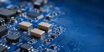
RF inductors are passive electrical components, crucial to the efficient operation of high-frequency circuits. At their core, they consist of a wire coil—wrapped around a specific core material (ceramic, ferrite, air)—which stores energy in a magnetic field when an electric current flows through. RF inductors differ from power inductors primarily in their response to high-frequency AC signals:
- Electromagnetic Principle: The fundamental theory is based on Faraday’s Law of Induction and Maxwell’s equations, where the coiled wire generates a concentrated magnetic field – the essence of its inductive properties.
- Frequency Domain Effects: At RF (3 kHz–300 GHz, wavelength down to 1 mm), the wavelength can be similar in scale to physical circuit elements, resulting in position-dependent voltages/currents.
- Skin Effect: At RF, the AC current migrates to the surface (“skin”) of the conductor, shrinking the effective cross-sectional area, increasing AC resistance, and reducing efficiency.
- Parasitics: Each real-world inductor has unintended stray capacitance, inductance, and resistive effects that become dominant at high frequencies.
Detailed: Key Parameters for Selection
| Parameter | Description | High-Frequency Impact | Insight |
|---|---|---|---|
| Inductance (L) | Magnitude of stored magnetic energy (L) | Defines reactance: X=2πfL | Higher frequency increases reactance; careful selection is crucial for filter and matching networks. |
| Self-Resonant Frequency (SRF) | Frequency where inductor’s own capacitance cancels its inductance | Above SRF: device acts as a capacitor, not an inductor | Golden rule: Always select inductors where SRF ≥ 10 × operating frequency to avoid failure in RF circuits. |
| Quality Factor (Q) | Ratio of stored energy vs. lost energy (Q=XR) | High Q = lower energy loss, sharper resonant filtering | Peak Q occurs below SRF; at higher frequencies, Q drops due to increased losses and skin effect. |
| DC Resistance (RDC) | Wire ohmic resistance | Lower RDC yields higher efficiency | Critical for battery-powered devices to minimize wasted power. |
| Current Rating | Maximum current before core saturation | Affects inductance stability | Consider not just for power inductors, but also for RF circuits that occasionally handle large currents. |
| Physical Size/Integration | Physical dimensions, SMD compatibility | Miniaturization can trade off with Q, SRF, current | Optimize package for fitting multi-frequency modules and compact modern devices. |
Technological Comparison and Insights
| Type | Material/Structure | Attributes | Challenges | Typical Applications |
|---|---|---|---|---|
| Wire-Wound (Ceramic/Ferrite) | Spiral copper wire around core | High Q, stable SRF, large current handling, low RDC, precise tolerance | Physically larger, expensive, parasitics limit performance at highest frequencies | RF filters, microwave circuits, matching networks, high-reliability systems |
| Multi-layer Ceramic | Printed spiral between ceramic layers | Ultra-compact, SMD friendly, high SRF, polarity marking for minimization of mutual coupling | Lower Q than wire-wound, value varies by side, higher RDC | Smartphones, IoT sensors, densely packed assemblies |
| Thin-Film | Photolithographically patterned | Exceptional precision, very high SRF, ultra-small, ideal for GHz+ operations | Narrow inductance range, cost, process complexity | High-frequency, mmWave, integrated RF modules |
| Air-Core | No core, just copper spiral | Highest Q, zero core loss, temperature stable, very large current | Bigger for high inductance, lower inductance/V, limited miniaturization | Broadband, impedance matching, I/O filtering |
Advanced Design: Parasitics and Performance Optimization
- Parasitic Capacitance: Each winding introduces capacitance, lowering SRF and risking capacitive behavior above resonance.
- Mutual Coupling: Orientation and proximity of multi-layer SMD inductors affect tolerance and signal interaction; polarity marking is significant for consistent performance.
- Core Materials: Ceramic (non-magnetic, stable, low loss), ferrite (higher permeability, more inductance, but core losses increase at high frequency), air (no losses, physical size increases).
- Skin Effect Management: At high frequency, select fine wires and optimized geometries to reduce AC resistance and maintain high Q.
- Plating Materials: Gold plating (maximal reliability, lowest losses, corrosion resistance); tin (cost-driven, higher losses, prone to oxidation).
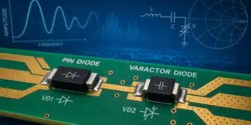
RF Inductor Applications and Real-World Roles
- Impedance Matching: Essential for maximum power transfer (e.g., amp-to-antenna), especially in multi-band RF front ends.
- Filtering: LC tanks, bandpass/bandstop filters—critical for signal selectivity, interference suppression, and regulatory compliance.
- Biasing/Choking: Allows DC current while blocking RF—must withstand DC and RF simultaneously.
- Resonance: Tuned with capacitors for oscillators and narrow-band circuits—Q and stability dictate ultimate precision.
Industry Trends and Design Challenges in Depth
- Miniaturization: Driving SMD technology, demanding both high-Q and very compact footprints.
- Ultra-high Frequency Support: Components specified and tested for 6 GHz+, supporting 5G and Wi-Fi 6E bands.
- Advanced Materials: Low-loss ceramics and novel compounds optimize Q and SRF in compact designs.
- Embedded Inductors: Integration directly into PCB substrate cuts parasitics, shrinks form factor, but demands manufacturing precision.
- AI/ML Automated Tuning: Adaptive matching networks use smart tunable inductors for optimal system performance in real time.
- Tolerance and Variability: Achieving ±2%–5% tolerance is complex as size shrinks, impacting yield and performance stability.
- Simulation and Modeling: Extremely accurate simulation models and S-parameter characterization are vital for predicting and verifying behaviors in the GHz domain.
Conclusion
RF inductors are the silent, critical elements ensuring the fidelity and performance of high-frequency designs. Selection must be an orchestrated balance between inductance, SRF, Q factor, and physical integration—especially as trends push towards higher frequencies and smaller form factors. Overcoming parasitic effects, achieving precision modeling, and leveraging advanced materials are essential to designing efficient, reliable RF circuits. Always operate well below SRF with the highest possible Q at your frequency of interest—the key indicators of successful RF inductor choice.
FAQ: RF Inductors in High-Frequency Design
RF inductors are passive electrical components that store energy in a magnetic field and are essential for high-frequency circuits (RF, microwave, 5G, IoT). They help manage signal integrity, impedance matching, and filtering in wireless devices whose performance is directly impacted by inductor characteristics.
Key selection parameters include inductance value, self-resonant frequency (SRF), quality factor (Q), DC resistance (RDC), current rating, and physical size/integration. These affect signal filtering, efficiency, power handling, and miniaturization capabilities.
The SRF marks the frequency where an inductor’s own parasitic capacitance dominates, turning its behavior capacitive rather than inductive. Operating above SRF can cause filtering and matching failures. The recommended practice is to select an SRF at least 10 times higher than the operating frequency.
Wire-wound inductors offer high Q and SRF, ideal for high-performance applications, but are larger and costlier. Multilayer inductors excel in miniaturization and SMD compatibility but have lower Q. Thin-film inductors deliver precision and highest SRF for GHz+ domains but at higher cost and with a narrower inductance range.
Polarity marking ensures tighter tolerance and consistent performance because the inductance may slightly vary depending on component orientation. It also reduces mutual coupling when placing inductors close together, supporting dense PCB layouts.
Engineers should recalibrate their vector network analyzer (VNA), check for fixture errors, and swap inductors with higher Q. If matching improves, an inductor issue was present; otherwise, analyze s-parameters and circuit layout for ground returns or unwanted couplings.
Gold plating delivers better corrosion resistance and lower losses, making it suitable for high-reliability designs; tin plating is more cost-effective for mass-market products but comes with higher losses and is more prone to oxidation.
How to Select the Optimal RF Inductor for Your High-Frequency Circuit
- Define your operating frequency and signal requirements
Identify the exact frequency range and required signal quality for your application. Consider filtering needs and power handling.
- List required electrical parameters
Determine desired inductance, minimum Q factor, SRF (should be at least 10× your highest operating frequency), RDC, and current rating. Assess integration and miniaturization needs.
- Match technology to performance and size requirements
Choose wire-wound for high Q/SRF and large currents, multilayer for compact SMD/IoT applications, or thin-film for GHz operations with tight precision.
- Consider material and plating choices
Select gold plating for high reliability and performance, or tin plating if cost constraints outweigh corrosion resistance.
- Simulate and verify with advanced modeling tools
Use accurate simulation and measurement (including S-parameters) to validate component choice and minimize parasitic effects and impedance mismatch.
- Prototype and test in real-world conditions
ssemble prototypes and evaluate performance metrics (Q, SRF) in target frequency bands, adjusting selection as required to optimize system efficiency and signal integrity.