
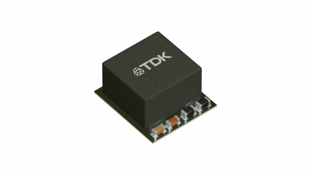
TDK has introduced the FS1525, a new member of its µPOL non‑isolated DC‑DC power module family delivering 25 A per module in a very low‑profile package.
The device targets high‑current, low‑voltage rails in AI servers, edge computing, telecom, and data center systems, with a particular focus on vertical power delivery directly under advanced processors. By stacking multiple modules, designers can scale current capability up to 200 A while keeping the power stage compact and thermally efficient.
Key features and benefits
The FS1525 is a complete point‑of‑load module integrating power stage, inductor, control, and digital management in a single compact package. It is designed to simplify high‑density board layouts while meeting demanding transient and noise requirements of modern AI and networking silicon.
- Continuous output current per module: 25 A, scalable to 200 A by stacking or paralleling multiple devices in interleaved operation.
- Very low profile: 3.82 mm height, suitable for placement under FPGAs/SoCs or ASICs on the backside of the PCB in vertical power delivery architectures.
- Compact footprint: 7.65 × 6.80 mm (L × W), enabling tight placement near high‑current loads and improved power density.
- Wide input range: 4.5 V to 16 V, covering typical 12 V intermediate bus and other common front‑end rails.
- Adjustable output voltage: 0.6 V to 1.8 V, optimized for core rails of 3 nm to 6 nm ASICs, FPGAs, SoCs, SERDES supplies, and similar low‑voltage loads.
- Operating temperature range: −40 °C to +125 °C, allowing use in harsh ambient conditions and thermally constrained systems.
- Ultra‑fast transient response and very low DC ripple, supporting aggressive dynamic load steps typical of AI and high‑speed digital workloads.
- Low spectral noise performance, suitable for sensitive DSP, imaging, and automated test equipment where conducted and radiated noise are critical.
- Integrated true differential remote sensing to regulate the voltage directly at the load pins and compensate for PCB trace drops.
- Pre‑bias capability, allowing the module to start safely into already pre‑charged outputs without disturbing existing rails.
For system designers, the main benefit is a high‑current PoL solution that behaves like a single component: no external compensation network is required, and the integrated inductor and MOSFETs remove a large part of the layout and selection effort typical of discrete buck converters.
Typical applications
The FS1525 is targeted at systems where board space, power density, and dynamic performance are key design constraints.
- AI and edge computing platforms, including inference accelerators and compact AI appliances where vertical power delivery frees space on the top side of the PCB.
- Data center and cloud servers, particularly for feeding AI accelerators, NICs, and high‑end FPGAs on PCIe and other plug‑in cards.
- Telecom and networking equipment, such as baseband units, routers, and switches that require tightly regulated low‑voltage rails at high current.
- Optical networks and high‑speed transceiver modules, where low spectral noise and tight regulation help maintain signal integrity.
- Medical imaging systems, which often combine high compute density with sensitive analog front ends, benefiting from low ripple and low noise rails.
- General power for AI chipsets, ASICs, FPGAs, and SoCs in form factors like PCIe cards, 1U–3U rack systems, VPX modules, SMARC, and similar high‑density standards.
In many of these applications, placing the power module on the backside of the PCB directly under the processor shortens current paths, improves transient behavior, and supports higher operating currents without increasing top‑side congestion.
Technical highlights
A key aspect of the FS1525 is its 3D chip‑embedded package technology, which integrates the entire buck converter into a single thermally optimized structure.
- Integration level: controller, driver, MOSFETs, digital core, memory banks, bypass capacitors, and power inductor are all embedded within the module’s 3D package.
- Thermal performance: the architecture achieves a thermal impedance of 1.4 K/W, supporting high current at elevated ambient temperatures and easing heatsinking design.
- Stackable architecture: modules can be paralleled or stacked to reach up to 200 A combined output, with active current sharing and interleaved operation up to 16 MHz to reduce input and output ripple.
- Digital interfaces: I²C and PMBus interfaces provide programmability and telemetry, including VIN, VOUT, IOUT, temperature, and fault reporting.
- Configuration storage: on‑board MTP (multi‑time programmable) memory stores custom device configurations, enabling system‑level power profiles.
- Analog VOUT settings: support for analog configuration of output voltages tailored to major FPGA/SoC and ASIC vendors, including support for Altera SmartVID on Agilex FPGA families.
- Vertical power delivery: the module is explicitly designed for mounting under the FPGA/SoC or ASIC on the PCB backside, reducing distance between power stage and load and improving both electrical and thermal performance.
For engineers, this means a high‑performance multiphase buck solution without the usual complexity of phase interleaving design, error amplifier compensation, and discrete magnetics selection. The module approach also helps standardize the power tree across different boards and product variants.
Design‑in notes for engineers
The FS1525 is best used as a close‑in PoL regulator for high‑current digital loads where transient behavior and space are critical. When designing in the module, several practical aspects should be considered.
- Vertical power delivery placement: the module is optimized to sit directly under the FPGA/SoC or ASIC, so work closely with the mechanical and PCB layout teams to ensure sufficient backside clearance, via fields for current paths, and appropriate thermal interfaces to chassis or heatsinks.
- Current scaling and thermal design: when stacking modules for 50 A, 100 A, or 200 A outputs, perform detailed thermal simulations and measurements, leveraging the specified 1.4 K/W thermal impedance and system‑level airflow assumptions from the datasheet.
- Power integrity and decoupling: although the module integrates key bypass capacitors, additional high‑frequency and bulk decoupling near the load will still be required; follow the manufacturer’s PDN recommendations and reference layouts for target FPGAs/SoCs.
- Remote sensing: use the true differential remote sense pins to connect directly to the load pads of the processor or ASIC to compensate for IR drops across vias and planes, especially in high‑current, low‑voltage designs.
- Digital configuration and monitoring: integrate the I²C/PMBus interface into the system controller or BMC to use telemetry (VIN, VOUT, IOUT, temperature) for closed‑loop power management, fault logging, and dynamic optimization of AI workloads.
- Start‑up and sequencing: take advantage of pre‑bias support and digital control to manage power‑up sequences with other rails; verify sequencing requirements from FPGA/SoC vendors such as Altera and AMD and map these into the FS1525 configuration.
- EMC considerations: the low spectral noise and interleaved operation help meet EMI limits, but layout discipline (short loops, solid return planes, controlled input filtering) remains essential; use the provided SIMPLIS models and PDN libraries to verify frequency‑domain behavior.
For many design teams, the plug‑and‑play nature of the FS1525 (no external compensation) and the availability of starter design files reduce the risk of first‑time‑right failures and accelerate the transition from prototype to production hardware.
Source
This article is based on information provided by TDK Corporation’s official press release and associated product documentation for the FS1525 µPOL power module, complemented by publicly available design collateral and product page information from the manufacturer.
References
- TDK press release: Power management products – FS1525 µPOL modules for up to 200 A vertical power delivery
- TDK product page – FS1525‑0600‑AL µPOL DC‑DC power module
- Ultra Librarian – FS1525 starter design schematics and PCB layout
- FS1525 SIMPLIS model and PDN libraries overview

