
Unverified or counterfeited electronic components pose a big threat globally because they could lead to malfunction of safety-critical systems and reduced reliability of high-hazard assets. Researchers at Cranfield University in UK propose a new fast non-destructive method of electronic components inspection using pulsed thermography.
Introduction
The current inspection techniques are either expensive or slow, which becomes the bottleneck of large volume inspection. As a complement of the existing inspection capabilities, a pulsed thermography-based screening technique is proposed in this paper using a digital twin methodology.
A FEM-based simulation unit is initially developed to simulate the internal structure of electronic components with deviations of multiple physical properties, informed by X-ray data, along with its thermal behaviour under exposure to instantaneous heat. A dedicated physical inspection unit is then integrated to verify the simulation unit and further improve the simulation by taking account of various uncertainties caused by equipment and samples. Principle component analysis is used for feature extraction, and then a set of machine learning-based classifiers are employed for quantitative classification. Evaluation results of 17 chips from different sources successfully demonstrate the effectiveness of the proposed technique.

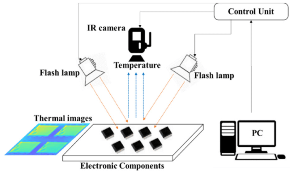
Among the diverse non-destructive testing (NDT) inspection methods, pulsed thermography (PT) – see Fig.1., is especially attractive for the inspection of UnVerified Electronic Components (UVECs) because it allows the inspection of a significant number of components simultaneously, facilitating a rapid and relatively low-cost inspection per part due to its rapid, non-contact inspection manner and its ability to produce intuitive inspection images.
Furthermore, a systematic investigation combined together with a simulation-based approach, can conveniently provide predictive insights of the PT detectability for the specific defect types in UVECs, thus remaining unascertained and scientifically worthwhile. This research addresses the challenge to identify UVECs with physical defects including the deviation of internal structures and material properties in the die, lead frame and the mould packaging which are typically found in the supply chain of ECs. For instance, components with undersized die and over-simplified lead frame from disqualified manufacturing are reported to be short-lived and incapable in electronic option. Besides, unsourced, low-cost and unqualified mould materials have been found in chips and have failed in long-term thermal fatigue cycles and ageing tests. It is therefore essential to clarify not only the inspection feasibility, but also which variability can be ascertained in PT thermography.
Counterfeit Inspection of Electronic Components
This research starts with inspection of a common type of electronic chip: operational amplifiers (OpAmps). A total of 17 OpAmps were collected from various trade markets to investigate their thermal responses in PT.

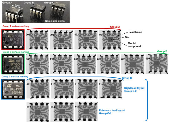
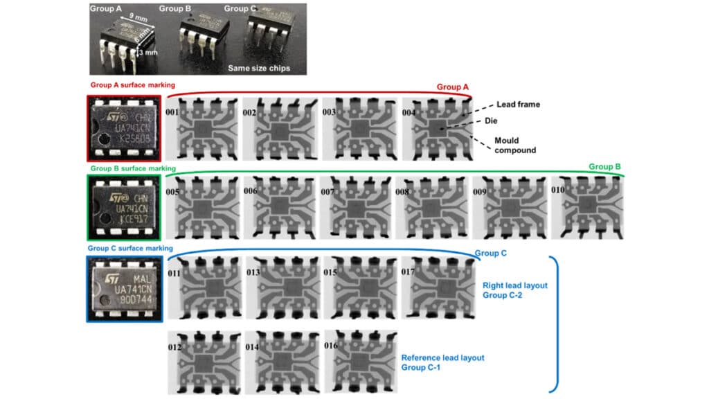
All samples are common dual in-line package chips and are designed for the same electronic purpose (e.g., UA741CN). They have almost identical external appearance except for surface markings. It should be noted that this study has no interest in investigating the surface labelling. To reveal the internal structure of these chips, X-ray inspection was adopted to obtain their lead frame and die details. The Figure 2 (also featured image) presents the exterior dimensions, surface markings, and X-Ray images of 17 samples, which can be categorised into three groups according to the surface markings.
Firstly, as shown by surface marking, chips of group A (from ‘001’ to ‘004’) and B (from ‘005’ to ‘010’) are from the same origin marked by “CHN” but those of Group C (from ‘011’ to ‘017’) are original from “MAL”. The markings of “UA741CN” suggest same electronic function. The ECs of Group B and C were tested by the electronic function testing and proven to be malfunctional or broken, while others in Group A were verified as sound ones.
Secondly, all chips were tested using the same X-ray inspection and the result of Group A is considered as the ground truth of the internal structure. The internal structure of the lead frame and die in Group A and B are consistent, while those in Group C exhibit variations in the lead frame layout, die position and size. The die of ‘011’, ‘013’, ‘015’ and ‘017’ appears to the right half of the chip while the die of ‘012’, ‘014’ and ‘016’ are positioned towards the left.
Additionally, based on the intensity in X-Ray images, chips in Group C have different mould materials, which is a common variability between manufacturers. Based on these preliminary information set, the strategies from both simulation modelling and experimental inspection are discussed below.
3D Modelling and Simulation
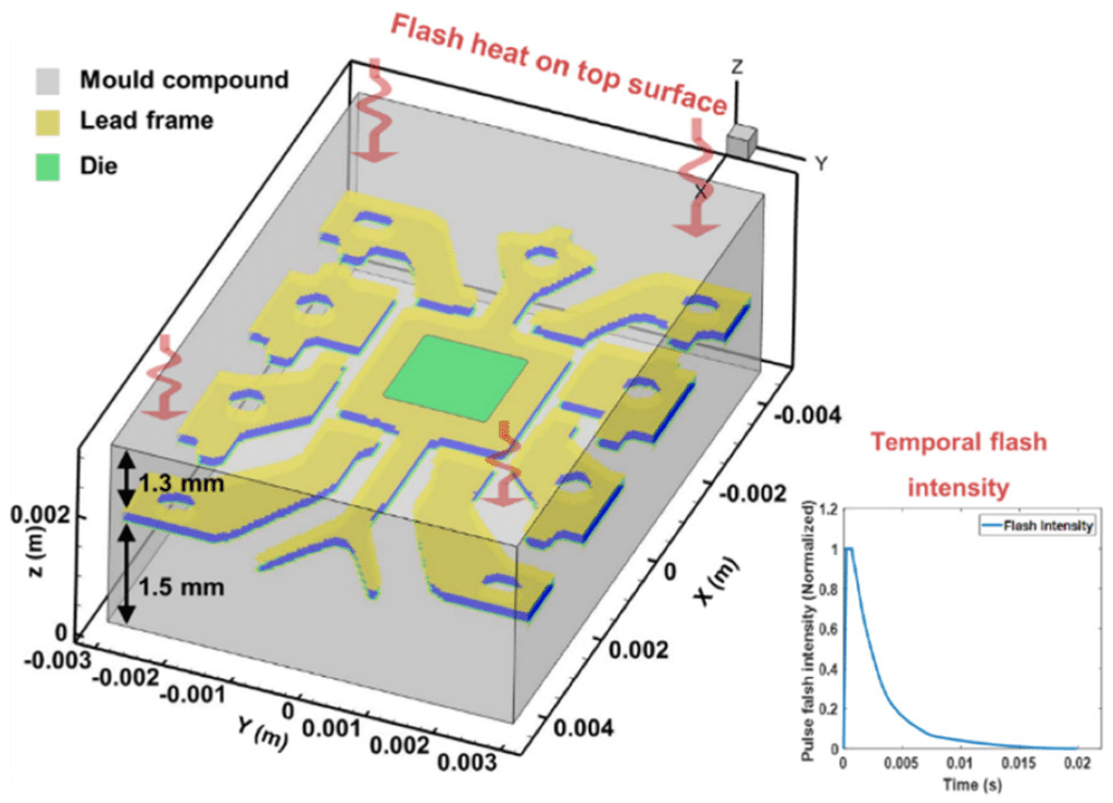
In this research, the electronic components are in a typical dual in-line packaged type which is mainly composed of multiple layers composed of three primary materials: mould, lead frame and die. To simulate the real structure of the EC, the X-ray images of verified chips are referenced to provide an accurate layout of the internal lead frame and die. According to the X-Ray images, the layout and dimension of the lead frame and die dimension are initially transferred to a binary mask. Then by mapping the mask onto the specific layers of the model, the real internal structure is simulated in the virtual environment. As a result, a 3D model is established with three layers with different materials, shown in Figure 3, including the mould compound layers, the lead frame layer and the die layer.
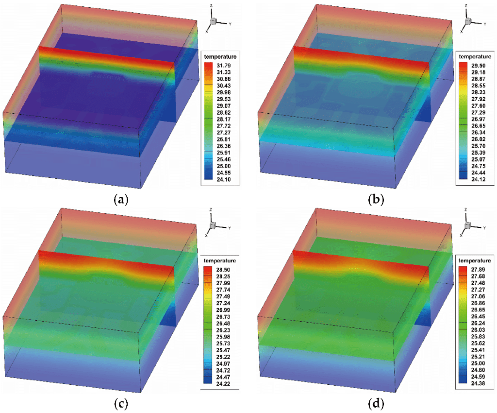
To investigate the transient temperature transfer, the verified component model and variation models were established and simulated. Figure 4 presents the temperature distributions of the verified component model (shown in Figure 3) at 0.04, 0.08, 0.12 and 0.16 s after the flash.


Conclusions
This paper reports a new UVEC inspection technique that includes the FEM simulation and experimental prototype, following the digital twin methodology. The simulation is able to model the complex internal structure of ECs, informed by X-ray images, and effectively predict the surface thermal behaviour after application of instantaneous heat.
The results suggest that the 2nd and 3rd peak of principal components of temperature delay profile can provide a sensitive and robust indication for the deviation of die size, lead frame layout and mould material properties. This research finding has been confirmed through using the same data analysis method for the experimental data, which were collected by a new established dedicated pulsed thermography prototype.
With the support of machine learning-based classifier, quantitative results suggest that the proposed technique can effectively identify the unverified components with certain robustness considering the variation of verified components. We also demonstrate that this technique can work under both single-inspection and batch-inspection modes, which offers the deployment flexibility to the supply chain.
The proposed technique can act as a powerful screening tool, after which other NDT techniques can be conducted on suspicious chips to improve the efficiency of UVEC inspection.
Future work in this area will extend the inspection scale of UVECs to establish a feature signal database of different types of UVECs. It will help both improving the simulation modelling of details in EC, upgrades to the versatility of the inspection system and significantly enhance the AI decision making strategy. In the feature selection approach, the EOFs in PCA will contain more spatial information of the ECs internal structure like lead and die layout which could enhance the inspection visualization. It will be investigated carefully in future.
See the full paper in the link below

