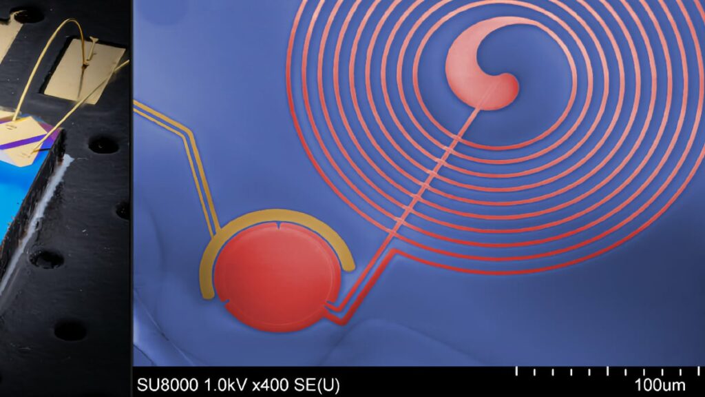
Researchers at TU Wien have developed a high‑aspect‑ratio superconducting vacuum gap capacitor NEMS structure with plate distances down to just 32 nm, setting a new benchmark for nano‑scale parallel‑plate capacitor technology in quantum electromechanics.
High‑Aspect‑Ratio Vacuum Gap Capacitor Concept
At the heart of the work is a parallel‑plate capacitor, in which the bottom aluminum electrode is fixed and the top aluminum electrode is realized as a free‑standing nanomembrane.
The capacitor is embedded into an LC resonant circuit via a planar spiral inductor, so that any motion of the membrane modulates the electrical resonance frequency and enables strong electromechanical coupling.
By engineering a vertical gap of only a few tens of nanometers across membrane radii from around 7 µm up to tens of micrometers, the device achieves a very high capacitance density and strong parametric coupling while maintaining mechanical stability.
Key Capacitor Metrics and Quantum‑Ready Performance
One of the central figures of merit is the parametric coupling rate between the membrane motion and the LC cavity, which scales inversely with the static capacitor gap.
By shrinking the rest‑position gap well below 50 nm, TU Wien significantly enhances the coupling, thereby increasing responsivity and reducing the required RF drive power for a given readout sensitivity.
At cryogenic temperatures around 400 mK, a device with an electrical resonance of about 1.29 GHz demonstrated an estimated plate separation of only 32 nm, confirmed by lumped‑element circuit simulations and RF characterisation.
Such gap dimensions and operation in the superconducting regime make these capacitors suitable for advanced quantum electromechanical experiments, including sideband cooling, squeezing, and potentially entanglement schemes when coupled to high‑Q mechanical modes.
Wafer‑Level Process for High‑Yield Capacitor Fabrication
A major advance of the TU Wien work lies in achieving wafer‑level, high‑yield fabrication of vacuum gap capacitors on standard silicon wafers using CMOS‑compatible thin‑film processes.
The stack is built from a stress‑compensated silicon oxide/silicon nitride substrate coating, a thin bottom aluminum electrode, a sputtered silicon sacrificial layer that defines the nanometer‑scale gap, and a top aluminum plate acting as both membrane and upper capacitor electrode.
In addition, a 300 nm aluminum nitride piezoelectric layer is integrated near the capacitor for on‑chip mechanical actuation, enabling controlled excitation of membrane eigenmodes without relying solely on capacitive driving.
Stress Engineering and Membrane Stability
Vacuum gap capacitors are inherently prone to failure due to collapse or buckling of the top electrode, so the TU Wien team placed strong emphasis on stress engineering.
Two critical issues were addressed: asymmetric oxidation of the top aluminum layer, and the vertical stress gradient across the membrane thickness created by sputter deposition.
To avoid asymmetric oxidation, a thin silicon capping layer is deposited immediately after the top aluminum in high vacuum, so that both sides of the membrane oxidize simultaneously only after release, creating balanced oxide layers and avoiding stress‑induced collapse.
To control the stress gradient, plasma power and chamber pressure during aluminum sputtering were systematically optimized; reducing power down to about 50 W at 3 µbar and using a high‑thermal‑capacity molybdenum holder minimized thermal load and yielded nearly constant average stress already at film thicknesses between roughly 40 and 60 nm.
This optimisation significantly reduced both buckling‑up (increased gap, lower coupling) and buckling‑down (gap closure, short circuits) scenarios, enabling a controlled trade‑off between coupling strength and fabrication yield.
Controlling Capacitor Gap at Cryogenic Temperatures
Because aluminum and silicon have very different thermal expansion coefficients, cooling from room temperature to millikelvin temperatures causes the aluminum membrane to contract more than the substrate and move closer to the bottom electrode.
Finite element simulations indicate gap reductions on the order of 120 nm for typical geometries when cooled from 300 K to 0 K, which must be accounted for in the sacrificial layer thickness and membrane slope design.
By tailoring the sacrificial silicon thickness, its lithographic undercut (which sets the membrane slope), and the average stress in the top electrode, the team ensured that devices maintain a safe but extremely small gap at operation temperature, reaching the targeted 32 nm without membrane collapse.
Yield and Scalability of Nano‑Gap Capacitors
With the optimized deposition and release process, TU Wien reports three wafers containing around 400 fully functional vacuum gap capacitors each, demonstrating true wafer‑level scalability.
Visual inspection combined with spot measurements using laser Doppler vibrometry showed room‑temperature yields above 90% for membrane radii comparable to those commonly used in the field, and around 50% even for larger radii.
These yields are particularly notable given the extreme aspect ratio of the capacitors and the very small target gaps, and they mark a substantial step towards practical sensing applications rather than single‑device laboratory demonstrations.
Electromechanical Characterisation of the Capacitor Membranes
At room temperature, the free‑standing aluminum membranes exhibit fundamental eigenfrequencies around a few MHz with quality factors on the order of several hundred in vacuum, verified using LDV measurements.
Using the integrated aluminum nitride piezoelectric actuator, higher vibrational modes can also be excited and mapped, demonstrating robust coupling between the actuator and the capacitor membrane structure.
At cryogenic temperatures, RF transmission measurements through the integrated spiral inductor and capacitor reveal well‑defined electrical resonances, and their dependence on drive power gives insight into nonlinear effects such as kinetic inductance and power‑dependent Q‑factor reduction.
Implications for Future Capacitor‑Based Quantum Metrology
The TU Wien results show that superconducting, high‑aspect‑ratio vacuum gap capacitors with nanometer‑scale plate distances can be realized in a scalable, silicon‑based process.
Such capacitors provide extremely strong parametric coupling in compact LC resonators, enabling sensitive displacement and force sensing, nonlinear bifurcation‑based readout schemes, and potential integration into circulators or directional amplifiers.
Combined with the high mechanical quality factors attainable in micro‑ and nano‑membranes, these devices form a robust platform for quantum electromechanics and for next‑generation quantum metrology tools, including ultra‑high‑resolution atomic force microscopy and quantum‑limited sensor architectures.
Source
This article is based on information from the official TU Wien press release and the corresponding peer‑reviewed article in Advanced Materials Technologies describing the development and fabrication of superconducting vacuum gap capacitor NEMS devices with plate distances down to 32 nm.
