
source: TDK application note
Recently released TDK application note compare chip capacitor and chip varistor ESD performance.
Electrostatic Countermeasure By Multilayer Ceramic Chip Capacitors
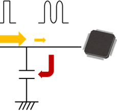
Protection components are used as an electrostatic countermeasure in equipment. Protection components are placed in circuits to protect ICs or electronic components, and to protect ICs or peripheral electronic components from static electricity that generate from places such as switches or headphone jacks. Protection components are largely divided into four categories: Zener diodes (TVS diodes), multilayer chip varistors (MLVs), ESD suppressors, and multilayer ceramic chip capacitors (MLCCs). When there is no limit for inserted capacitance, MLCCs are often used.
Since the electrostatic absorption capacity of a MLCC becomes greater as the capacitance becomes larger, components with a larger capacitance are selected. However, if changes such as switching to an IC with a faster communication speed are made due to a design change by the end user. The signal waveform may be distorted due to the effect of large capacitance (Fig. 1). If the MLCC is switched to one with smaller capacity so as to improve this, electrostatic countermeasure may become insufficient. In such a case, it is necessary to choose protection components other than MLCCs.
This material describes the characteristics of each protection component, as well as the differences between an MLCC and MLV.
Communication speed: Low Communication speed: High


Fig. 1 Signal waveform distortion due to difference in communication speed
Characteristics of Each Protection Component Used as ESD Countermeasures
In order to protect semiconductor devices or circuits from surges including ESD, protection components such as multilayer ceramic chip capacitors, ESD suppressors, TVS diodes, and MLVs are used. The characteristics of these protection components are summarized below (Table 1).
Table 1 Features of each protection component
| Type | L x W size | Capacitance(pF) | Features | |||
|---|---|---|---|---|---|---|
| 1 or lower | 1 to 50 | 50 to 100 | 100 or higher | |||
| MLV | 0.4mm x 0.2mm [EIA01005] or larger |
✓ | ✓ | ✓ |
|
|
| TVS diode | 0.6mm x 0.3mm [EIA0201] or larger |
✓ | ✓ | ✓ |
|
|
| ESD suppressor | 0.6mm x 0.3mm [EIA0201] or larger |
✓ |
|
|||
| MLCC (for ESD Protection) |
1.6mm x 0.8mm [EIA0603] or larger |
✓ |
|
|||


- When no protection component is used (ESD simulator charge voltage 8 kV, 150 pF, 330Ω, contact discharge), the pulse surge shows a waveform in which the voltage value gradually decreases after a steep rise of the initial peak voltage. The peak voltage (Vpeak) reaches as high as 1,500 V, and the average voltage (Vave) between 30 ns and 100 ns is also as high as 400 V.
- An ESD suppressor is a type of protection component that forms a short circuit at a specified voltage when the applied voltage is gradually increased, and suddenly allows the current to flow. This voltage is called the trigger voltage. Although an ESD suppressor can suppress Vave to 29 V, it can only suppress Vpeak to approximately 500 V due to the high trigger voltage.
- An MLCC suppresses voltage by charging the ESD electric charge with its capacitance component. Therefore, the larger the capacitance, the greater the ESD suppression capability. An MLCC is capable of suppressing Vpeak to approximately 23 V. However, since it later discharges accumulated charges, a large voltage peak will be generated a several hundred nanoseconds later.
- A TVS diode is a protection component derived from a Zener diode (constant voltage diode) used for ESD countermeasure. It is also called a transient voltage suppressor. Its ESD absorption waveform shows excellent properties, with low Vpeak and Vave.
- An MLV also shows a waveform having low Vpeak and Vave, as in the case of a TVS diode. In addition, since an MLV has a capacitance component, it has an advantage over a TVS diode in suppressing Vpeak. However, in MLVs, the ESD suppression capability tends to become worse as the capacitance becomes larger; therefore, in high-speed signal circuits in which large capacitance cannot be inserted, TVS diodes show superior properties.
Fig. 3 shows a map of the best-suited protection component for each application. The horizontal axis represents the signal speed, and the vertical axis represents the electrostatic absorption performance. In addition, the communication speed of each standard is shown in the lower part. Using this graph, the best suited protection component can be selected for each standard. MLCCs can be used in signal lines with a signal speed of 1Mbps or less. In signal lines with higher speeds, chip varistors, TVS diodes, or ESD suppressors are suitable. As is indicated by Fig. 3, there are AVRM series and AVRL series chip varistors of TDK. The AVRM series features high capacitance and high electrostatic absorption capability, realizing electrostatic absorption in signal lines with speeds from 10kbps to 100Mbps. On the other hand, the AVRL series features low capacitance, and exhibits a higher electrostatic absorption capacity than that of ESD suppressors in high frequencies approximately from 50Mbps to 1Gbps.
A chip protector features low capacitance and high electrostatic absorption capability, and is suitable as a replacement for TVS diodes. It shows even higher electrostatic absorption capability than, not only an ESD suppressor, but the AVRL series at communication speeds from approximately 10Mbps to 1Gbps.


Fig. 3 Map of the best suited protection component for each applicationChip varistors are available in the AVRM series and AVRL series.
The features of the AVRM series are high capacitance and high electrostatic absorption capability. In communication lines between 10kbps and 10Mbps, products in this series can achieve high electrostatic absorption. They can be used for applications including LIN and CAN in automobiles and in audio, video, mics, switches, and SIM card parts.
On the other hand, the feature of the AVRL series is low capacitance. As a result, in faster transmission lines between 50Mbps and 1Gbps, products in this series demonstrate higher electrostatic absorption than ESD suppressors.
Faster systems such as USB, LVDS, MIPI, and HDMI and automotive applications such as MOST, PoDL, and Ethernet are optimal applications including.
The features of chip protectors are low capacitance and high electrostatic absorption capability, and they are suitable as replacements for TVS diodes.
In transmission lines between 50Mbps and 500Mbps, chip protectors demonstrate electrostatic absorption which is not only higher than ESD suppressors, but even higher than the AVRL series.
The CGA3EA series of chip capacitors, which specializes in high electrostatic absorption, is suitable for use as an ESD protection measure at relatively low transmission lines of 1Mbps or less.
Differences in the ESD absorption waveform depending on the capacitance
The electrostatic absorption capability of MLCCs differ largely by their capacitance size. The higher the capacitance, the greater the electrostatic absorption capability. The ESD absorption waveforms of MLCCs by their capacitance size are shown in Fig. 4.


Based on IEC61000-4-2, a 4kV ESD waveform was generated using an HBM (Human Body Model) and the electrostatic absorption capabilities of each protection components were evaluated. The horizontal axis represents time (ns), and the vertical axis represents voltage (V). The peak voltage was 662V with a 100pF MLCC, 350V with a 1000 pF MLCC, 155V with a 10nF MLCC, and 10V with a 100nF MLCC. The 100nF MLCC showed a very high static electricity absorption capability. However, 100nF MLCCs often cause distortion of signal waveforms and cannot be used in communication lines other than power lines. On the other hand, if the capacitance of an MLCC is decreased down to 100pF, it will lose almost all its electrostatic absorption capability, even though it can be used in audio or video lines from the perspective of communication speed. Therefore, for electrostatic countermeasures in communication lines other than power lines, protection components other than MLCCs need to be used.
Electrostatic absorption capability of an MLCC and MLV having the same capacitance
Fig. 5 shows the ESD absorption waveforms of an MLCC and MLV having the same capacitance. This graph is also based on IEC61000-4-2, a 4kV ESD waveform was generated using an HBM (Human Body Model) and the electrostatic absorption capabilities of each protection components were evaluated.


The peak voltage was as low as 37 V with an MLV, while it was 662 V with an MLCC. As was previously described, an MLCC accumulates electricity inside the element when static electricity is applied. For this reason, a large capacitance is required in order to obtain a high electrostatic absorption capability. On the other hand, an MLV has a property in which the resistance of the element itself decreases when overvoltage is applied, and thus does not require high capacitance. When the capacitance is the same, an MLV has a much higher electrostatic protection capability compared to an MLCC. Therefore, when MLCCs cannot be used due to a restriction by capacitance, it is recommended that MLVs be used.
Selection Point for MLVs
The key points for selecting MLVs as a electrostatic countermeasure are described in the following. The primary focus should be given to increasing the ESD endurance of equipment. By selecting a product with the lowest varistor voltage to the extent possible, an excellent electrostatic absorption capability can be obtained; however, it is necessary to select an optimum value according to the circuit voltage value. In addition, when the varistor voltage is the same, the electrostatic absorption capability and electrostatic durability becomes greater as the capacitance becomes larger. However, the signal quality deteriorates as the capacitance becomes larger, as in the case of an MLCC; therefore, a product with the largest capacitance that will not affect the signal quality should be selected. The product lineup of the chip varistors of TDK is shown in Table 2.
| Series | LxW size | Max. Operating Voltage [DC](V) |
Varistor voltage [@1mA](V) |
Capacitance (pF) |
Supported Communication Speed |
|---|---|---|---|---|---|
| AVRM series | 0.4 x 0.2 to 2.0 x 1.2mm [EIA01005 to EIA0805] |
3.5 to 28 | 6.8 to 39 | 15 to 1050 | 10kbps to 100Mbps |
| AVRL series | 0.4 x 0.2 to 1.6 x 0.8mm [EIA01005 to EIA0805] |
10 to 25 | 27 to 90 | 0.5 to 6.8 | 50Mbps to 1Gbps |
| SGNE series | 0.4 x 0.2 to 0.6 x 0.3mm [EIA01005 to EIA0201] |
4.3 to 15 | 8 to 27 | 6.8 to 15 | 50Mbps to 500Mbps |

