
This presentation by René Linde, Field Application Engineer at Würth Elektronik published by All About Circuits discusses PCB design challenges of connector and interconnection technologies.
The presentation explores the mechanical, electrical, and design challenges associated with these components, offering insights into best practices for layout, testing, and integration.
Introduction
Modern PCB design increasingly relies on electromechanical components that offer high reliability, mechanical stability, and electrical performance.
Technologies such as press-fit terminals, SKEDD connectors, and SMA interfaces are reshaping how engineers approach solderless connections, impedance matching, and high-frequency signal integrity.
Press-fit contacts enable solder-free, mechanically stable connections directly to the PCB and are particularly suitable for current-carrying applications. Complementing this, SKEDD technology offers a tool-free plug-in solution with a 2.54 mm pitch that eliminates the need for soldering, simplifying assembly and enhancing system reliability. Multiboard designs, whether board-to-board, wire-to-board, or board-to-wire, require precise interface planning. Changes to a connector can have immediate effects on other PCBs. Accurate 3D placement of boards and cables supports mechanical integration and facilitates alignment with the housing.
Key Points
- Press-fit terminals provide gas-tight, solderless connections with superior mechanical and electrical reliability.
- SKEDD connectors enable tool-free, reusable connections with minimal PCB deformation.
- Impedance matching for SMA connectors requires precise taper geometry and simulation-driven layout optimization.
- Clearance and creepage distances are critical for high-voltage PCB safety and must be carefully managed.
- Mechanical reinforcement of SMD connectors can significantly improve push-pull force performance.
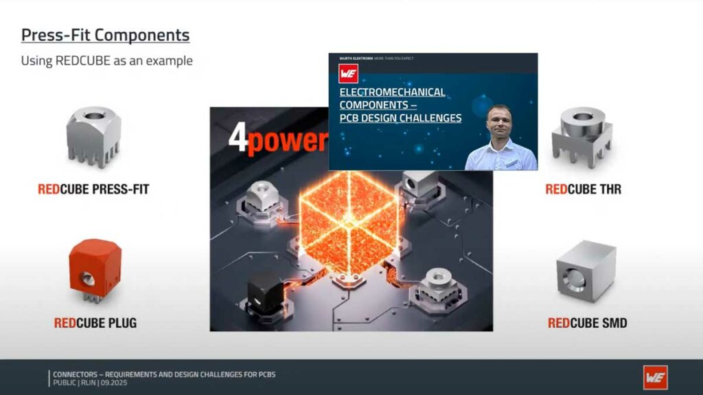
Press-Fit Technology and Cold Welding
Press-fit terminals, such as RedCube, utilize a cold welding mechanism where the pin is forcibly inserted into a plated via. This creates a gas-tight bond between brass and copper, eliminating the need for soldering. The optimal via diameter post-plating is approximately 1.475 mm, with copper thickness between 30–40 μm.
| Parameter | Recommended Value |
|---|---|
| Drill Hole Diameter | 1.66 mm |
| Copper Plating Thickness | 30–40 μm |
| Tin Layer Thickness | 2–15 μm |
| Final Via Diameter | 1.475 mm |
Extraction force per pin can reach up to 100 N, depending on PCB thickness and surface finish. Cold welding ensures lower resistance than soldered joints and prevents oxidation.
SKEDD Connectors: Reusable Solderless Interfaces
Unlike press-fit, SKEDD connectors use elastic fork contacts that do not permanently deform the via. They support multiple mating cycles—up to 50 for debugging and 10 for permanent layouts. This makes them ideal for modular and serviceable designs.
Impedance Matching for SMA Connectors
High-frequency applications require precise impedance matching between PCB traces and SMA connectors. A curved line taper geometry is used to transition from 50 Ω to 25 Ω impedance, minimizing signal loss.
The taper is divided into segments of quarter-wavelength multiples:
Where:
- λ = Wavelength
- c = Speed of light
- f = Frequency
- εr = Relative permittivity
Simulation-driven layout optimization using Altium Designer’s DXF import ensures accurate geometry replication. Modified layouts show reduced insertion loss and improved VSWR across 6–14 GHz.
Clearance and Creepage in High-Voltage Design
To prevent arcing and breakdown, clearance (air gap) and creepage (surface path) must be optimized. Slots and grooves in the PCB increase effective distances. Pollution degree and altitude influence required spacing.
| Pollution Degree | Minimum Clearance (mm) | Minimum Creepage (mm) |
|---|---|---|
| 1 | 0.6 | 1.0 |
| 2 | 1.0 | 2.5 |
| 3 | 1.5 | 4.0 |
Use of insulating barriers and strategic cutouts can extend creepage paths and improve safety margins.
Mechanical Reinforcement of SMD Connectors
Push-pull force testing reveals that standard SMD layouts offer limited mechanical stability. Modified layouts such as the “Mickey Mouse” footprint or via-reinforced pads significantly improve performance.
| Layout Type | Push Force (kg) | Pull Force (kg) |
|---|---|---|
| THT Datasheet | 75 | 50 |
| SMD Standard | 20 | 11 |
| Mickey Mouse | 37 | 20 |
| SMD with Vias | 35 | 19 |
Adhesive reinforcement can further increase pull resistance, though solder joint integrity remains the limiting factor.
Multiboard Integration and 3D Alignment
Multiboard systems require precise 3D alignment and connector planning. Using nominal models in Altium Designer, engineers can simulate mechanical fit and ensure housing compatibility. Spacer and basket connectors facilitate modular stacking.
Conclusion
Electromechanical components are no longer passive elements—they define the mechanical, electrical, and thermal boundaries of modern PCB design. By mastering press-fit techniques, impedance matching, and mechanical reinforcement, engineers can build robust, scalable systems. Simulation, measurement, and layout optimization are essential tools in this evolving landscape. As technologies like SKEDD and RedCube mature, they offer compelling alternatives to traditional soldering, paving the way for more efficient and reliable electronics.


